|
|

This appendix lists the pinouts for the cables you can use with the Cisco 1005 router.
Table A-1 lists the pinouts for the 10BaseT port.
| Pin | Description |
|---|---|
| 1 | TX+ |
| 2 | TX- |
| 3 | RX+ |
| 4 | - |
| 5 | - |
| 6 | RX- |
| 7 | - |
| 8 | - |
Table A-2 lists the pinouts for a straight-through 10BaseT cable, which is used to connect the router to an Ethernet hub.
| RJ-45 Pin | Signal | Direction | RJ-45 Pin |
|---|---|---|---|
| 1 | TX+ | --> | 1 |
| 2 | TX- | --> | 2 |
| 3 | RX+ | <-- | 3 |
| 4 | - | - | 4 |
| 5 | - | - | 5 |
| 6 | RX- | <-- | 6 |
| 7 | - | - | 7 |
| 8 | - | - | 8 |
Table A-3 lists the pinouts for a crossover 10BaseT cable, which is used to connect the router to an Ethernet network interface card.
| RJ-45 Pin | Signal | Direction | RJ-45 Pin | Signal |
|---|---|---|---|---|
| 1 | TX+ | --> | 3 | RX+ |
| 2 | TX- | --> | 6 | RX- |
| 3 | RX+ | <-- | 1 | TX+ |
| 4 | - | - | 4 | - |
| 5 | - | - | 5 | - |
| 6 | RX- | <-- | 2 | TX- |
| 7 | - | - | 7 | - |
| 8 | - | - | 8 | - |
The EIA/TIA-232 console port is configured as data terminal equipment (DTE) and uses an RJ-45 connector. A console cable kit is provided with your router to connect a console (an ASCII terminal or PC running terminal emulation software) to the console port. The console cable kit contains an RJ-45-to-RJ-45 roll-over cable and a RJ-45-to-DB-25 female DTE adapter (labeled "Terminal"). Table A-4 lists the pinouts for the asynchronous serial console port, the RJ-45-to-RJ-45 roll-over cable, and the RJ-45-to-DB-25 female DTE adapter.
| Console Port (DTE) | RJ-45-to-RJ-45 Roll-Over Cable | |||
|---|---|---|---|---|
| Signal | RJ-45 Pin | RJ-45 Pin | DB-25 Pin | Signal |
| - | 1 | 8 | 4 | - |
| DTR | 2 | 7 | 20 | DSR |
| TxD | 3 | 6 | 2 | RxD |
| GND | 4 | 5 | 7 | GND |
| GND | 5 | 4 | 7 | GND |
| RxD | 6 | 3 | 3 | TxD |
| DSR | 7 | 3 | 6 | DTR |
| - | 8 | 1 | 5 | - |
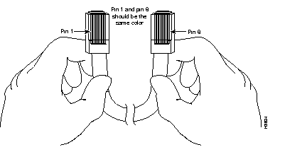
You can identify a roll-over cable by comparing the two modular ends of the cable. (See Figure A-1.) Holding the cables in your hand, side-by-side, with the tab at the back, the wire connected to the pin on the outside of the left connector (pin 1) should be the same color as the pin on the outside of the right connector (pin 8). On Cisco cables, pin 1 is white on one connector, and pin 8 is white on the other connector.
The serial port on the router uses a universal port, a 60-pin receptacle that supports the following serial interfaces: EIA/TIA-232, EIA/TIA-449, X.21, V.35, and EIA-530. The shielded serial transition cable determines the electrical interface type. The router end of all of the cables is a 60-pin connector.
DTE connectors have a plug connector at the network end. (DCE connectors have a receptacle at the network end.) However, V.35 is available in DTE mode with a connector of either gender at the network end. The serial port operates in DTE mode only.
The tables that follow list the signal pinouts for the DTE mode serial transition cables for each router interface type.
Figure A-2 shows the EIA/TIA-232 serial cable assembly, and Table A-5 lists the EIA/TIA-232 cable pinouts.
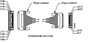
| 60 Pin1 | Signal | Description | Direction | 25 Pin | Signal |
|---|---|---|---|---|---|
| J1-50 J1-51 J1-52 | MODE_0 GND MODE_DCE | Shorting group | - | - | - |
| J1-46 | Shield GND | Single | - | J2-1 | Shield GND |
| J1-41 Shield | TxD/RxD - | Twisted pair no. 5 | --> - | J2-2 Shield | TxD - |
| J1-36 Shield | RxD/TxD - | Twisted pair no. 9 | <-- - | J2-3 Shield | RxD - |
| J1-42 Shield | RTS/CTS - | Twisted pair no. 4 | --> - | J2-4 Shield | RTS - |
| J1-35 Shield | CTS/RTS - | Twisted pair no. 10 | <-- - | J2-5 Shield | CTS - |
| J1-34 Shield | DSR/DTR - | Twisted pair no. 11 | <-- - | J2-6 Shield | DSR - |
| J1-45 Shield | Circuit GND - | Twisted pair no. 1 | - - | J2-7 Shield | Circuit GND - |
| J1-33 Shield | DCD/LL - | Twisted pair no. 12 | <-- - | J2-8 Shield | DCD - |
| J1-37 Shield | TxC/NIL - | Twisted pair no. 8 | <-- - | J2-15 Shield | TxC - |
| J1-38 Shield | RxC/TxCE - | Twisted pair no. 7 | <-- - | J2-17 Shield | RxC - |
| J1-44 Shield | LL/DCD - | Twisted pair no. 2 | --> - | J2-18 Shield | LTST - |
| J1-43 Shield | DTR/DSR - | Twisted pair no. 3 | --> - | J2-20 Shield | DTR - |
| J1-39 Shield | TxCE/TxC - | Twisted pair no. 6 | --> - | J2-24 Shield | TxCE - |
Figure A-3 shows the EIA/TIA-449 serial cable assembly, and Table A-6 lists the EIA/TIA-449 cable pinouts.
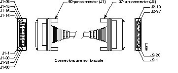
| 60 Pin2 | Signal | Description | Direction | 37 Pin | Signal |
|---|---|---|---|---|---|
| J1-49 J1-48 | MODE_1 GND | Shorting group | - | - | - |
| J1-51 J1-52 | GND MODE_DCE | Shorting group | - | - | - |
| J1-46 | Shield_GND | Single | _ | J2-1 | Shield GND |
| J1-11 J1-12 | TxD/RxD+ TxD/RxD- | Twisted pair no. 6 | --> --> | J2-4 J2-22 | SD+ SD- |
| J1-24 J1-23 | TxC/RxC+ TxC/RxC- | Twisted pair no. 9 | <-- <-- | J2-5 J2-23 | ST+ ST- |
| J1-28 J1-27 | RxD/TxD+ RxD/TxD- | Twisted pair no. 11 | <-- <-- | J2-6 J2-24 | RD+ RD- |
| J1-9 J1-10 | RTS/CTS+ RTS/CTS- | Twisted pair no. 5 | --> --> | J2-7 J2-25 | RS+ RS- |
| J1-26 J1-25 | RxC/TxCE+ RxC/TxCE- | Twisted pair no. 10 | <-- <-- | J2-8 J2-26 | RT+ RT- |
| J1-1 J1-2 | CTS/RTS+ CTS/RTS- | Twisted pair no. 1 | <-- <-- | J2-9 J2-27 | CS+ CS- |
| J1-44 J1-45 | LL/DCD Circuit_GND | Twisted pair no. 12 | --> _ | J2-10 J2-37 | LL SC |
| J1-3 J1-4 | DSR/DTR+ DSR/DTR- | Twisted pair no. 2 | <-- <-- | J2-11 J2-29 | DM+ DM- |
| J1-7 J1-8 | DTR/DSR+ DTR/DSR- | Twisted pair no. 4 | --> --> | J2-12 J2-30 | TR+ TR- |
| J1-5 J1-6 | DCD/DCD+ DCD/DCD- | Twisted pair no. 3 | <-- <-- | J2-13 J2-31 | RR+ RR- |
| J1-13 J1-14 | TxCE/TxC+ TxCE/TxC- | Twisted pair no. 7 | --> --> | J2-17 J2-35 | TT+ TT- |
| J1-15 J1-16 | Circuit_GND Circuit_GND | Twisted pair no. 9 | - - | J2-19 J2-20 | SG RC |
Figure A-4 shows the X.21 cable assembly, and Table A-7 lists the X.21 cable pinouts.
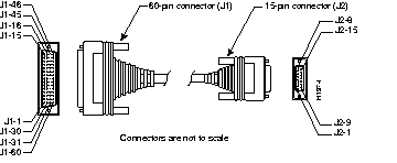
| 60 Pin3 | Signal | Description | Direction | 15 Pin | Signal |
|---|---|---|---|---|---|
| J1-48 J1-47 | GND MODE_2 | Shorting group | - | - | - |
| J1-51 J1-52 | GND MODE_DCE | Shorting group | - | - | - |
| J1-46 | Shield_GND | Single | - | J2-1 | Shield GND |
| J1-11 J1-12 | TxD/RxD+ TxD/RxD- | Twisted pair no. 3 | --> --> | J2-2 J2-9 | Transmit+ Transmit- |
| J1-9 J1-10 | RTS/CTS+ RTS/CTS- | Twisted pair no. 2 | --> --> | J2-3 J2-10 | Control+ Control- |
| J1-28 J1-27 | RxD/TxD+ RxD/TxD- | Twisted pair no. 6 | <-- <-- | J2-4 J2-11 | Receive+ Receive- |
| J1-1 J1-2 | CTS/RTS+ CTS/RTS- | Twisted pair no. 1 | <-- <-- | J2-5 J2-12 | Indication+ Indication- |
| J1-26 J1-25 | RxC/TxCE+ RxC/TxCE- | Twisted pair no. 5 | <-- <-- | J2-6 J2-13 | Timing+ Timing- |
| J1-15 Shield | Control_GND - | Twisted pair no. 4 | - - | J2-8 Shield | Control GND - |
Figure A-5 shows the V.35 cable assembly and Table A-8 lists the V.35 cable pinouts.
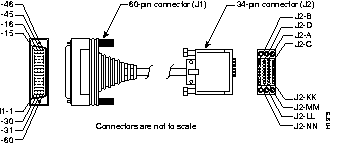
| 60 Pin4 | Signal | Description | Direction | 34 Pin | Signal |
|---|---|---|---|---|---|
| J1-49 J1-48 | MODE_1 GND | Shorting group | - | - | - |
| J1-50 J1-51 J1-52 | MODE_0 GND MODE_DCE | Shorting group | - | - | - |
| J1-53 J1-54 J1-55 J1-56 | TxC/NIL RxC_TxCE RxD/TxD GND | Shorting group | - | - | - |
| J1-46 | Shield_GND | Single | - | J2-A | Frame GND |
| J1-45 Shield | Circuit_GND - | Twisted pair no. 12 | - - | J2-B Shield | Circuit GND - |
| J1-42 Shield | RTS/CTS - | Twisted pair no. 9 | --> - | J2-C Shield | RTS - |
| J1-35 Shield | CTS/RTS - | Twisted pair no. 8 | <-- - | J2-D Shield | CTS - |
| J1-34 Shield | DSR/DTR - | Twisted pair no. 7 | <-- - | J2-E Shield | DSR - |
| J1-33 Shield | DCD/LL - | Twisted pair no. 6 | <-- - | J2-F Shield | RLSD - |
| J1-43 Shield | DTR/DSR - | Twisted pair no. 10 | --> - | J2-H Shield | DTR - |
| J1-44 Shield | LL/DCD - | Twisted pair no. 11 | --> - | J2-K Shield | LT - |
| J1-18 J1-17 | TxD/RxD+ TxD/RxD- | Twisted pair no. 1 | --> --> | J2-P J2-S | SD+ SD- |
| J1-28 J1-27 | RxD/TxD+ RxD/TxD- | Twisted pair no. 5 | <-- <-- | J2-R J2-T | RD+ RD- |
| J1-20 J1-19 | TxCE/TxC+ TxCE/TxC- | Twisted pair no. 2 | --> --> | J2-U J2-W | SCTE+ SCTE- |
| J1-26 J1-25 | RxC/TxCE+ RxC/TxCE- | Twisted pair no. 4 | <-- <-- | J2-V J2-X | SCR+ SCR- |
| J1-24 J1-23 | TxC/RxC+ TxC/RxC- | Twisted pair no. 3 | <-- <-- | J2-Y J2-AA | SCT+ SCT- |
Figure A-6 shows the EIA-530 cable assembly, and Table A-9 lists the EIA-530 DTE cable pinouts.
60 Pin5 | Signal | 25 Pin | Signal | Direction DTE DCE1 |
|---|---|---|---|---|
| J1-11 J1-12 | TxD/RxD+ TxD/RxD- | J2-2 J2-14 | BA(A), TxD+ BA(B), TxD- | --> --> |
| J1-28 J1-27 | RxD/TxD+ RxD/TxD- | J2-3 J2-16 | BB(A), RxD+ BB(B), RxD- | <-- <-- |
| J1-9 J1-10 | RTS/CTS+ RTS/CTS- | J2-4 J2-19 | CA(A), RTS+ CA(B), RTS- | --> --> |
| J1-1 J1-2 | CTS/RTS+ CTS/RTS- | J2-5 J2-13 | CB(A), CTS+ CB(B), CTS- | <-- <-- |
| J1-3 J1-4 | DSR/DTR+ DSR/DTR- | J2-6 J2-22 | CC(A), DSR+ CC(B), DSR- | <-- <-- |
| J1-46 J1-47 | Shield_GND MODE_2 | J2-1 - | Shield - | Shorted |
| J1-48 J1-49 | GND MODE_1 | - - | - - | Shorted |
| J1-5 J1-6 | DCD/DCD+ DCD/DCD- | J2-8 J2-10 | CF(A), DCD+ CF(B), DCD- | <-- <-- |
| J1-24 J1-23 | TxC/RxC+ TxC/RxC- | J2-15 J2-12 | DB(A), TxC+ DB(B), TxC- | <-- <-- |
| J1-26 J1-25 | RxC/TxCE+ RxC/TxCE- | J2-17 J2-9 | DD(A), RxC+ DD(B), RxC- | <-- <-- |
| J1-44 J1-45 | LL/DCD Circuit_GND | J2-18 J2-7 | LL Circuit_ GND | --> - |
| J1-7 J1-8 | DTR/DSR+ DTR/DSR- | J2-20 J2-23 | CD(A), DTR+ CD(B), DTR- | --> --> |
| J1-13 J1-14 | TxCE/TxC+ TxCE/TxC- | J2-24 J2-11 | DA(A), TxCE+ DA(B), TxCE- | --> --> |
|
|