|
|

This appendix provides the following pinout information:
Figure D-1 shows the management card console cable, and Table D-1 lists the pinouts.
Figure D-1 Management Card Console Cable
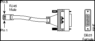
Table D-1 Management Card Console Port Pinouts
| RJ-45 Pins | Description | DB-25 Female Pins |
|---|---|---|
| 1 | RxD | 3 |
| 2 | GND | 7 |
| -- | CTS | 5(1) |
| -- | RTS | 41 |
| 8 | TxD | 2 |
Following are the pinouts for the router card auxiliary port (Table D-2), and the router card console port (Table D-3):
Table D-2 Router Card Auxiliary Port Pinouts (RJ-45)
| Auxiliary Port | ||
|---|---|---|
| Pin | Signal | Input/Output |
| 1 | RTS | Output |
| 2 | DTR | Output |
| 3 | TXD | Output |
| 4 | GND | -- |
| 5 | GND | -- |
| 6 | RXD | Input |
| 7 | DSR | Input |
| 8 | CTS | Input |
Table D-3 Router Card Console Port Pinouts (RJ-45)
| Console Port | ||
|---|---|---|
| Pin | Signal | Input/Output |
| 1 | -- | -- |
| 2 | DTR | Output |
| 3 | TxD | Output |
| 4 | GND | -- |
| 5 | GND | -- |
| 6 | RxD | Input |
| 7 | DSR | Input |
| 8 | -- | -- |
Refer to Table D-4 for a list of the pins used on the RJ-45 connector, the male/female DTE adapter, the male/female DCE adapter, and the male modem adapter used to connect terminals and modems to the Cisco hub. The connection of pins between the RJ-45 connector and the end device depends on the type of cable used, either straight or rolled. A straight cable connects pin 1 to pin 1, pin 2 to pin 2, and so on. A rolled cable connects pin 1 to pin 8, pin 2 to pin 7, and so on. The Cisco 2517 and Cisco 2519 ships with a rolled cable. Refer to Table D-5 for the cable and adapter configurations that can be used to connect terminals and modems to the Cisco 2517.
Table D-4 Pins for the RJ-45 Connector, M/F DTE, M DCE, and MMOD Adapters
| Cable | DB-25 Adapters | ||
|---|---|---|---|
| RJ-45 Pins | M/F DTE Pins(1) | M DCE Pins | MMOD Pins(2) |
| 1 | 4 | 5 | 5 |
| 2 | 20 | 6 | 8 |
| 3 | 2 | 3 | 3 |
| 4 | 7 | 7 | 7 |
| 5 | 7 | 7 | 7 |
| 6 | 3 | 2 | 2 |
| 7 | 6 | 20 | 20 |
| 8 | 5 | 4 | 4 |
Table D-5 Connection Configuration
| Router Card Port | RJ-45 Cable Type | DB-25 Adapter | End Device |
|---|---|---|---|
| Console/auxiliary | Rolled | FDTE | Terminal |
| Console/auxiliary | Straight | FDCE | Terminal |
| Console/auxiliary | Rolled | MDCE(1) | Modem |
| Console/auxiliary | Straight | MDTE1 | Modem |
| Auxiliary/console | Rolled | MMOD1 | Modem |
Table D-6 lists the router card BRI port pinout and signals.
Table D-6 BRI Port Pinout (RJ-45)
| Pin(1) | TE(2) | NT(3) | Polarity |
|---|---|---|---|
| 3 | Transmit | Receive | + |
| 4 | Receive | Transmit | + |
| 5 | Receive | Transmit | -- |
| 6 | Transmit | Receive | -- |
![]()
Table D-7 lists the pinout for the Token Ring interface ports.
Table D-7 Token Ring Port Pinout (RJ-45)
| RJ-45 Pins | Signal |
|---|---|
| 1 | GND |
| 2 | GND |
| 3 | Tx |
| 4 | Rx |
| 5 | Tx |
| 6 | Rx |
| 7 | GND |
| 8 | Not used |
The following illustrations and tables provide assembly drawings and pinouts for the EIA-530 DCE, and EIA/TIA-232, EIA/TIA-449, V.35, and X.21 DTE and DCE cables.
Figure D-2 shows the EIA-530 serial cable assembly, and Table D-8 lists the pinouts. Arrows indicate signal direction: ---> indicates DTE to DCE, and <--- indicates DCE to DTE.
Figure D-2 EIA-530 Serial Cable Assembly
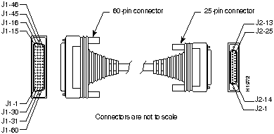
Table D-8 EIA-530 DTE Cable Pinout (DB-60 to DB-25)
| 60 Pin(1) | Signal | 25 Pin | Signal | DirectionDTE DCE(2) |
|---|---|---|---|---|
| J1-1J1-2 | CTS/RTS+CTS/RTS-- | J2-5J2-13 | CB(A), CTS+ CB(B), CTS-- | <---<--- |
| J1-3J1-4 | DSR/DTR+DSR/DTR-- | J2-6J2-22 | CC(A), DSR+ CC(B), DSR-- | <---<--- |
| J1-5J1-6 | DCD/DCD+DCD/DCD-- | J2-8J2-10 | CF(A), DCD+CF(B), DCD-- | <---<--- |
| J1-7J1-8 | DTR/DSR+DTR/DSR-- | J2-20J2-23 | CD(A), DTR+CD(B), DTR-- | --->---> |
| J1-9J1-10 | RTS/CTS+RTS/CTS-- | J2-4J2-19 | CA(A), RTS+CA(B), RTS-- | --->---> |
| J1-11J1-12 | TxD/RxD+TxD/RxD-- | J2-2J2-14 | BA(A), TxD+BA(B), TxD-- | --->---> |
| J1-13J1-14 | TxCE/TxC+TxCE/TxC-- | J2-24J2-11 | DA(A), TxCE+DA(B), TxCE-- | --->---> |
| J1-24J1-23 | TxC/RxC+TxC/RxC-- | J2-15J2-12 | DB(A), TxC+DB(B), TxC-- | <---<--- |
| J1-26J1-25 | RxC/TxCE+RxC/TxCE-- | J2-17J2-9 | DD(A), RxC+DD(B), RxC-- | <---<--- |
| J1-28J1-27 | RxD/TxD+RxD/TxD-- | J2-3J2-16 | BB(A), RxD+BB(B), RxD-- | <---<--- |
| J1-44J1-45 | LL/DCDCircuit_GND | J2-18J2-7 | LL Circuit_ GND | --->-- |
| J1-46J1-47 | Shield_GNDMODE_2 | J2-1-- | Shield-- | Shorted |
| J1-48J1-49 | GNDMODE_1 | ---- | ---- | Shorted |
| J1-51J1-52 | GNDMODE_DCE | ---- | ---- | Shorted |
Figure D-3 shows the EIA/TIA-232 cable assembly; Table D-9 lists the DTE pinout; and Table D-10 lists the DCE pinout. Arrows indicate signal direction: ---> indicates DTE to DCE, and <--- indicates DCE to DTE.
Figure D-3 EIA/TIA-232 Cable Assembly

Table D-9 EIA/TIA-232 DTE Cable Pinout (DB-60 to DB-25)
| 60 Pin(1) | Signal | Description | Direction | 25 Pin | Signal |
|---|---|---|---|---|---|
| J1-50J1-51J1-52 | MODE_0GNDMODE_DCE | Shorting group | -- | -- | -- |
| J1-46 | Shield GND | Single | -- | J2-1 | Shield GND |
| J1-41Shield | TxD/RxD-- | Twisted pair no. 5 | --->-- | J2-2Shield | TxD-- |
| J1-36Shield | RxD/TxD-- | Twisted pair no. 9 | <----- | J2-3Shield | RxD-- |
| J1-42Shield | RTS/CTS-- | Twisted pair no. 4 | --->-- | J2-4Shield | RTS-- |
| J1-35Shield | CTS/RTS-- | Twisted pair no. 10 | <----- | J2-5Shield | CTS-- |
| J1-34Shield | DSR/DTR-- | Twisted pair no. 11 | <----- | J2-6Shield | DSR-- |
| J1-45Shield | Circuit GND-- | Twisted pair no. 1 | ---- | J2-7Shield | Circuit GND-- |
| J1-33Shield | DCD/LL-- | Twisted pair no. 12 | <----- | J2-8Shield | DCD-- |
| J1-37Shield | TxC/NIL-- | Twisted pair no. 8 | <----- | J2-15Shield | TxC-- |
| J1-38Shield | RxC/TxCE-- | Twisted pair no. 7 | <----- | J2-17Shield | RxC-- |
| J1-44Shield | LL/DCD-- | Twisted pair no. 2 | --->-- | J2-18Shield | LTST-- |
| J1-43Shield | DTR/DSR-- | Twisted pair no. 3 | --->-- | J2-20Shield | DTR-- |
| J1-39Shield | TxCE/TxC-- | Twisted pair no. 6 | --->-- | J2-24Shield | TxCE-- |
Table D-10 EIA/TIA-232 DCE Cable Pinout (DB-60 to DB-25)
| 60 Pin(1) | Signal | Description | Direction | 25 Pin | Signal |
|---|---|---|---|---|---|
| J1-50J1-51 | MODE_0GND | Shorting group | -- |
-- |
-- |
| J1-46 | Shield GND | Single | -- | J2-1 | Shield GND |
| J1-36Shield | RxD/TxD-- | Twisted pair no. 9 | <----- | J2-2Shield | TxD-- |
| J1-41Shield | TxD/RxD-- | Twisted pair no. 5 | --->-- | J2-3Shield | RxD-- |
| J1-35Shield | CTS/RTS-- | Twisted pair no. 10 | <----- | J2-4Shield | RTS-- |
| J1-42Shield | RTS/CTS-- | Twisted pair no. 4 | --->-- | J2-5Shield | CTS-- |
| J1-43Shield | DTR/DSR-- | Twisted pair no. 3 | --->-- | J2-6Shield | DSR-- |
| J1-45Shield | Circuit GND-- | Twisted pair no. 1 | ---- | J2-7Shield | Circuit GND |
| J1-44Shield | LL/DCD-- | Twisted pair no. 2 | --->-- | J2-8Shield | DCD-- |
| J1-39Shield | TxCE/TxC-- | Twisted pair no. 7 | --->-- | J2-15Shield | TxC-- |
| J1-40Shield | NIL/RxC-- | Twisted pair no. 6 | --->-- | J2-17Shield | RxC-- |
| J1-33Shield | DCD/LL-- | Twisted pair no. 12 | <----- | J2-18Shield | LTST-- |
| J1-34Shield | DSR/DTR-- | Twisted pair no. 11 | <----- | J2-20Shield | DTR-- |
| J1-38Shield | RxC/TxCE-- | Twisted pair no. 8 | <----- | J2-24Shield | TxCE-- |
Figure D-4 shows the EIA/TIA-449 cable assembly; Table D-11 lists the DTE pinout, and Table D-12 lists the DCE pinout. Arrows indicate signal direction: ---> indicates DTE to DCE, and <--- indicates DCE to DTE.
Figure D-4 EIA/TIA-449 Cable Assembly
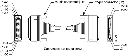
Table D-11 EIA/TIA-449 DTE Cable Pinout (DB-60 to DB-37)
| 60 Pin(1) | Signal | Description | Direction | 37 Pin | Signal |
|---|---|---|---|---|---|
| J1-49J1-48 | MODE_1GND | Shorting group | -- | -- | -- |
| J1-51J1-52 | GNDMODE_DCE | Shorting group | -- | -- | -- |
| J1-46 | Shield_GND | Single | _ | J2-1 | Shield GND |
| J1-11J1-12 | TxD/RxD+TxD/RxD-- | Twisted pair no. 6 | --->---> | J2-4J2-22 | SD+SD-- |
| J1-24J1-23 | TxC/RxC+TxC/RxC-- | Twisted pair no. 9 | <---<--- | J2-5J2-23 | ST+ST-- |
| J1-28J1-27 | RxD/TxD+RxD/TxD-- | Twisted pair no. 11 | <---<--- | J2-6J2-24 | RD+RD-- |
| J1-9J1-10 | RTS/CTS+RTS/CTS-- | Twisted pair no. 5 | --->---> | J2-7J2-25 | RS+RS-- |
| J1-26J1-25 | RxC/TxCE+RxC/TxCE-- | Twisted pair no. 10 | <---<--- | J2-8J2-26 | RT+RT-- |
| J1-1J1-2 | CTS/RTS+CTS/RTS-- | Twisted pair no. 1 | <---<--- | J2-9J2-27 | CS+CS-- |
| J1-44J1-45 | LL/DCDCircuit_GND | Twisted pair no. 12 | --->_ | J2-10J2-37 | LLSC |
| J1-3J1-4 | DSR/DTR+DSR/DTR-- | Twisted pair no. 2 | <---<--- | J2-11J2-29 | DM+DM-- |
| J1-7J1-8 | DTR/DSR+DTR/DSR-- | Twisted pair no. 4 | --->---> | J2-12J2-30 | TR+TR-- |
| J1-5J1-6 | DCD/DCD+DCD/DCD-- | Twisted pair no. 3 | <---<--- | J2-13J2-31 | RR+RR-- |
| J1-13J1-14 | TxCE/TxC+TxCE/TxC-- | Twisted pair no. 7 | --->---> | J2-17J2-35 | TT+TT-- |
| J1-15J1-16 | Circuit_GNDCircuit_GND | Twisted pair no. 9 | ---- | J2-19J2-20 | SGRC |
Table D-12 EIA/TIA-449 DCE Cable Pinout (DB-60 to DB-37)
| 60 Pin(1) | Signal | Description | Direction | 37 Pin | Signal |
|---|---|---|---|---|---|
| J1-49J1-48 | MODE_1GND | Shorting group | -- | -- | -- |
| J1-46 | Shield_GND | Single | -- | J2-1 | Shield GND |
| J1-28J1-27 | RxD/TxD+RxD/TxD-- | Twisted pair no. 11 | <---<--- | J2-4J2-22 | SD+SD-- |
| J1-13J1-14 | TxCE/TxC+TxCE/TxC-- | Twisted pair no. 7 | --->---> | J2-5J2-23 | ST+ST-- |
| J1-11J1-12 | TxD/RxD+TxD/RxD-- | Twisted pair no. 6 | --->---> | J2-6J2-24 | RD+RD-- |
| J1-1J1-2 | CTS/RTS+CTS/RTS-- | Twisted pair no. 1 | <---<--- | J2-7J2-25 | RS+RS-- |
| J1-24J1-23 | TxC/RxC+TxC/RxC-- | Twisted pair no. 9 | --->---> | J2-8J2-26 | RT+RT-- |
| J1-9J1-10 | RTS/CTS+RTS/CTS-- | Twisted pair no. 5 | --->---> | J2-9J2-27 | CS+CS-- |
| J1-29J1-30 | NIL/LLCircuit_GND | Twisted pair no. 12 | --->-- | J2-10J2-37 | LLSC |
| J1-7J1-8 | DTR/DSR+DTR/DSR-- | Twisted pair no. 4 | --->---> | J2-11J2-29 | DM+DM-- |
| J1-3J1-4 | DSR/DTR+DSR/DTR-- | Twisted pair no. 2 | <---<--- | J2-12J2-30 | TR+TR-- |
| J1-5J1-6 | DCD/DCD+DCD/DCD-- | Twisted pair no. 3 | --->---> | J2-13J2-31 | RR+RR-- |
| J1-26J1-25 | RxC/TxCE+RxC/TxCE-- | Twisted pair no. 10 | <---<--- | J2-17J2-35 | TT+TT-- |
| J1-15J1-16 | Circuit_GNDCircuit_GND | Twisted pair no. 8 | __ | J2-19J2-20 | SGRC |
Figure D-5 shows the V.35 cable assembly; Table D-13 lists the DTE pinout, and Table D-14 lists the DCE pinout. Arrows indicate signal direction: ---> indicates DTE to DCE, and <--- indicates DCE to DTE.
Figure D-5 V.35 Cable Assembly
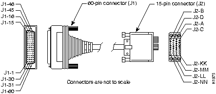
Table D-13 V.35 DTE Cable Pinout (DB-60 to 34-Pin)
| 60 Pin(1) | Signal | Description | Direction | 34 Pin | Signal |
|---|---|---|---|---|---|
| J1-49J1-48 | MODE_1GND | Shorting group | -- | -- | -- |
| J1-50J1-51J1-52 | MODE_0GNDMODE_DCE | Shorting group | -- | -- | -- |
| J1-53J1-54J1-55J1-56 | TxC/NILRxC_TxCERxD/TxDGND | Shorting group | -- | -- | -- |
| J1-46 | Shield_GND | Single | -- | J2-A | Frame GND |
| J1-45Shield | Circuit_GND-- | Twisted pair no. 12 | ---- | J2-BShield | Circuit GND-- |
| J1-42Shield | RTS/CTS-- | Twisted pair no. 9 | --->-- | J2-CShield | RTS-- |
| J1-35Shield | CTS/RTS-- | Twisted pair no. 8 | <----- | J2-DShield | CTS-- |
| J1-34Shield | DSR/DTR-- | Twisted pair no. 7 | <----- | J2-EShield | DSR-- |
| J1-33Shield | DCD/LL-- | Twisted pair no. 6 | <----- | J2-FShield | RLSD-- |
| J1-43Shield | DTR/DSR-- | Twisted pair no. 10 | --->-- | J2-HShield | DTR-- |
| J1-44Shield | LL/DCD-- | Twisted pair no. 11 | --->-- | J2-KShield | LT-- |
| J1-18J1-17 | TxD/RxD+TxD/RxD-- | Twisted pair no. 1 | --->---> | J2-PJ2-S | SD+SD-- |
| J1-28J1-27 | RxD/TxD+RxD/TxD-- | Twisted pair no. 5 | <---<--- | J2-RJ2-T | RD+RD-- |
| J1-20J1-19 | TxCE/TxC+TxCE/TxC-- | Twisted pair no. 2 | --->---> | J2-UJ2-W | SCTE+SCTE-- |
| J1-26J1-25 | RxC/TxCE+RxC/TxCE-- | Twisted pair no. 4 | <---<--- | J2-VJ2-X | SCR+SCR-- |
| J1-24J1-23 | TxC/RxC+TxC/RxC-- | Twisted pair no. 3 | <---<--- | J2-YJ2-AA | SCT+SCT-- |
Table D-14 V.35 DCE Cable Pinout (DB-60 to 34-Pin)
| 60 Pin(1) | Signal | Description | Direction | 34 Pin | Signal |
|---|---|---|---|---|---|
| J1-49J1-48 | MODE_1GND | Shorting group | -- | -- | -- |
| J1-50J1-51 | MODE_0GND | Shorting group | -- | -- | -- |
| J1-53J1-54J1-55J1-56 | TxC/NILRxC_TxCERxD/TxDGND | Shorting group | -- | -- | -- |
| J1-46 | Shield_GND | Single | -- | J2-A | Frame GND |
| J1-45Shield | Circuit_GND-- | Twisted pair no. 12 | ---- | J2-BShield | Circuit GND-- |
| J1-35Shield | CTS/RTS-- | Twisted pair no. 8 | <----- | J2-CShield | RTS-- |
| J1-42Shield | RTS/CTS-- | Twisted pair no. 9 | --->-- | J2-DShield | CTS-- |
| J1-43Shield | DTR/DSR-- | Twisted pair no. 10 | --->-- | J2-EShield | DSR-- |
| J1-44Shield | LL/DCD-- | Twisted pair no. 11 | --->-- | J2-FShield | RLSD-- |
| J1-34Shield | DSR/DTR-- | Twisted pair no. 7 | <----- | J2-HShield | DTR-- |
| J1-33Shield | DCD/LL-- | Twisted pair no. 6 | <----- | J2-KShield | LT-- |
| J1-28J1-27 | RxD/TxD+RxD/TxD-- | Twisted pair no. 5 | <---<--- | J2-PJ2-S | SD+SD-- |
| J1-18J1-17 | TxD/RxD+TxD/RxD-- | Twisted pair no. 1 | --->---> | J2-RJ2-T | RD+RD-- |
| J1-26J1-25 | RxC/TxCE+RxC/TxCE-- | Twisted pair no. 4 | <---<--- | J2-UJ2-W | SCTE+SCTE-- |
| J1-22J1-21 | NIL/RxC+NIL/RxC-- | Twisted pair no. 3 | --->---> | J2-VJ2-X | SCR+SCR-- |
| J1-20J1-19 | TxCE/TxC+TxCE/TxC-- | Twisted pair no. 2 | --->---> | J2-YJ2-AA | SCT+SCT-- |
Figure D-6 shows the X.21 cable assembly; Table D-15 lists the DTE pinout, and Table D-16 lists the DCE pinout. Arrows indicate signal direction: ---> indicates DTE to DCE, and <--- indicates DCE to DTE.
Figure D-6 X.21 Cable Assembly
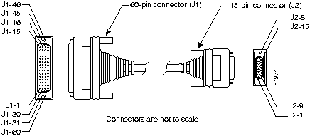
Table D-15 X.21 DTE Cable Pinout (DB-60 to DB-15)
| 60 Pin(1) | Signal | Description | Direction | 15 Pin | Signal |
|---|---|---|---|---|---|
| J1-48J1-47 | GNDMODE_2 | Shorting group | -- | -- | -- |
| J1-51J1-52 | GNDMODE_DCE | Shorting group | -- | -- | -- |
| J1-46 | Shield_GND | Single | -- | J2-1 | Shield GND |
| J1-11J1-12 | TxD/RxD+TxD/RxD-- | Twisted pair no. 3 | --->---> | J2-2J2-9 | Transmit+Transmit-- |
| J1-9J1-10 | RTS/CTS+RTS/CTS-- | Twisted pair no. 2 | --->---> | J2-3J2-10 | Control+Control-- |
| J1-28J1-27 | RxD/TxD+RxD/TxD-- | Twisted pair no. 6 | <---<--- | J2-4J2-11 | Receive+Receive-- |
| J1-1J1-2 | CTS/RTS+CTS/RTS-- | Twisted pair no. 1 | <---<--- | J2-5J2-12 | Indication+Indication-- |
| J1-26J1-25 | RxC/TxCE+RxC/TxCE-- | Twisted pair no. 5 | <---<--- | J2-6J2-13 | Timing+Timing-- |
| J1-15Shield | Control_GND-- | Twisted pair no. 4 | ---- | J2-8Shield | Control GND-- |
Table D-16 X.21 DCE Cable Pinout (DB-60 to DB-15)
| 60 Pin(1) | Signal | Description | Direction | 15 Pin | Signal |
|---|---|---|---|---|---|
| J1-48J1-47 | GNDMODE_2 | Shorting group | -- | -- | -- |
| J1-46 | Shield_GND | Single | -- | J2-1 | Shield GND |
| J1-28J1-27 | RxD/TxD+RxD/TxD-- | Twisted pair no. 6 | <---<--- | J2-2J2-9 | Transmit+Transmit-- |
| J1-1J1-2 | CTS/RTS+CTS/RTS-- | Twisted pair no. 1 | <---<--- | J2-3J2-10 | Control+Control-- |
| J1-11J1-12 | TxD/RxD+TxD/RxD-- | Twisted pair no. 3 | --->---> | J2-4J2-11 | Receive+Receive-- |
| J1-9J1-10 | RTS/CTS+RTS/CTS-- | Twisted pair no. 2 | --->---> | J2-5J2-12 | Indication+Indication-- |
| J1-24J1-23 | TxC/RxC+TxC/RxC-- | Twisted pair no. 4 | --->---> | J2-6J2-13 | Timing+Timing-- |
| J1-15Shield | Control_GND-- | Twisted pair no. 5 | ---- | J2-8Shield | Control GND-- |
|
|
Copyright 1988-1995 © Cisco Systems Inc.