|
|
This appendix describes cable signals and pinouts.
The cables available from us meet Federal Communications Commission (FCC) part 15J Class B requirements and Verband Deutscher Electrotechniker (VDE) 0871 Limit B levels. When constructing your own cables, refer to applicable standards for regulatory compliance, interference considerations, and cable length limitations.
Following are the signal summaries contained in this appendix:
The EIA/TIA-232 console port is configured as DTE and uses an RJ-45 connector.
The router ships with a cable kit to connect a console (an ASCII terminal or PC running terminal emulation software) to the console port. The console cable kit contains an RJ-45-to-RJ-45 rollover cable and RJ-45-to-DB-9 and RJ-45-to-DB-25 female DTE adapters (labeled Terminal). Table C-1 lists pinouts for the asynchronous serial console port and auxiliary port, the RJ-45-to-RJ-45 rollover cable, and the RJ-45-to-DB-9 and RJ-45-to-DB-25 female DTE adapters.
| Auxiliary and Console Port (DTE) | RJ-45-to-RJ-45 Rollover Cable | RJ-45-to-DB-9 Adapter | RJ-45-to-DB-25 Adapter | ||
|---|---|---|---|---|---|
| Signal | RJ-45 Pin | RJ-45 Pin | DB-9 Pin | DB-25 Pin | Signal |
| RTS | 1 | 8 | 8 | 5 | CTS |
| DTR | 2 | 7 | 6 | 6 | DSR |
| TxD | 3 | 6 | 2 | 3 | RxD |
| GND | 4 | 5 | 5 | 7 | GND |
| GND | 5 | 4 | 5 | 7 | GND |
| RxD | 6 | 3 | 3 | 2 | TxD |
| DSR | 7 | 2 | 4 | 20 | DTR |
| CTS | 8 | 1 | 7 | 4 | RTS |
You can identify a rollover cable by comparing the modular plugs at the two ends of the cable. When you hold the plugs side by side, with the tab at the back, the wire connected to the pin on the outside of the left plug should be the same color as the wire connected to the pin on the outside of the right plug. (See Figure C-1.) If you purchased your cable from Cisco Systems, pin 1 is white on one connector, and pin 8 is white on the other (a rollover cable connects pins 1 and 8, 2 and 7, 3 and 6, and 4 and 5).
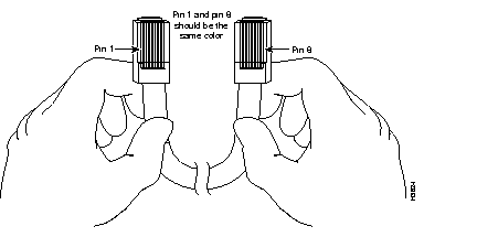
Table C-1 and Table C-2 list the signal pinouts for both the DTE-mode and DCE-mode serial port adapter cables for each serial interface type.
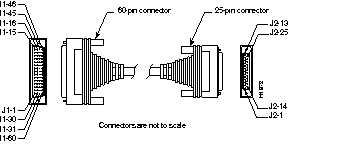
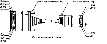
Figure C-2 shows the EIA/TIA-232 serial cable assembly. Table C-2 lists the DTE pinouts, and Table C-3 lists the DCE pinouts. Arrows indicate signal direction: --> indicates DTE to DCE, and <-- indicates DCE to DTE.
| 60 Pin | Signal | Note | Direction | 25 Pin | Signal |
|---|---|---|---|---|---|
| J1-50
J1-51 J1-52 | MODE_0
GND MODE_DCE | Shorting group | - | - | - |
| J1-46 | Shield GND | Single | - | J2-1 | Shield GND |
| J1-46 | Shield GND | Single | - | J2-1 | Shield GND |
| J1-41
Shield | TXD/RXD
- | Twisted pair no. 5 | -->
- | J2-2
Shield | TXD
- |
| J1-36
Shield | RXD/TXD
- | Twisted pair no. 9 | <--
- | J2-3
Shield | RXD
- |
| J1-42
Shield | RTS/CTS
- | Twisted pair no. 4 | -->
- | J2-4
Shield | RTS
- |
| J1-35
Shield | CTS/RTS
- | Twisted pair no. 10 | <--
- | J2-5
Shield | CTS
- |
| J1-34
Shield | DSR/DTR
- | Twisted pair no. 11 | <--
- | J2-6
Shield | DSR
- |
| J1-45
Shield | Circuit GND
- | Twisted pair no. 1 | -
- | J2-7
Shield | Circuit GND
- |
| J1-33
Shield | DCD/LL
- | Twisted pair no. 12 | <--
- | J2-8
Shield | DCD
- |
| J1-37
Shield | TXC/NIL
- | Twisted pair no. 8 | <--
- | J2-15
Shield | TXC
- |
| J1-38
Shield | RXC/TXCE
- | Twisted pair no. 7 | <--
- | J2-17
Shield | RXC
- |
| J1-44
Shield | LL/DCD
- | Twisted pair no. 2 | -->
- | J2-18
Shield | LTST
- |
| J1-43
Shield | DTR/DSR
- | Twisted pair no. 3 | -->
- | J2-20
Shield | DTR
- |
| J1-39
Shield | TXCE/TXC
- | Twisted pair no. 6 | -->
- | J2-24
Shield | TXCE
- |
| 60 Pin | Signal | Note | Direction | 25 Pin | Signal |
|---|---|---|---|---|---|
| J1-50 J1-51 | MODE_0 GND | Shorting group | - | - | - |
| J1-36 Shield | RXD/TXD - | Twisted pair no. 9 | <-- - | J2-2 Shield | TXD - |
| J1-41 Shield | TXD/RXD - | Twisted pair no. 5 | --> - | J2-3 Shield | RXD - |
| J1-35 Shield | CTS/RTS - | Twisted pair no. 10 | <-- - | J2-4 Shield | RTS - |
| J1-42 Shield | RTS/CTS - | Twisted pair no. 4 | --> - | J2-5 Shield | CTS - |
| J1-43 Shield | DTR/DSR - | Twisted pair no. 3 | --> - | J2-6 Shield | DSR - |
| J1-45 Shield | Circuit GND - | Twisted pair no. 1 | - - | J2-7 Shield | Circuit GND |
| J1-44 Shield | LL/DCD - | Twisted pair no. 2 | --> - | J2-8 Shield | DCD - |
| J1-39 Shield | TXCE/TXC - | Twisted pair no. 7 | --> - | J2-15 Shield | TXC - |
| J1-40 Shield | NIL/RXC - | Twisted pair no. 6 | --> - | J2-17 Shield | RXC - |
| J1-33 Shield | DCD/LL - | Twisted pair no. 12 | <-- - | J2-18 Shield | LTST - |
| J1-34 Shield | DSR/DTR - | Twisted pair no. 11 | <-- - | J2-20 Shield | DTR - |
| J1-38 Shield | RXC/TXCE - | Twisted pair no. 8 | <-- - | J2-24 Shield | TXCE - |
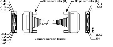
Figure C-3 shows the EIA/TIA-449 serial cable assembly. Table C-4 lists the DTE pinouts, and Table C-5 lists the DCE pinouts. Arrows indicate signal direction: --> indicates DTE to DCE, and <-- indicates DCE to DTE.
| 60 Pin | Signal Name | Note | Direction | 37 Pin | Signal Name |
|---|---|---|---|---|---|
| J1-49 J1-48 | MODE_1 GND | Shorting group | - | - | - |
| J1-51 J1-52 | GND MODE_DCE | Shorting group | - | - | - |
| J1-46 | Shield_GND | Single | _ | J2-1 | Shield GND |
| J1-11 J1-12 | TXD/RXD+ TXD/RXD- | Twisted pair no. 6 | --> --> | J2-4 J2-22 | SD+ SD- |
| J1-24 J1-23 | TXC/RXC+ TXC/RXC- | Twisted pair no. 9 | <-- <-- | J2-5 J2-23 | ST+ ST- |
| J1-28 J1-27 | RXD/TXD+ RXD/TXD- | Twisted pair no. 11 | <-- <-- | J2-6 J2-24 | RD+ RD- |
| J1-9 J1-10 | RTS/CTS+ RTS/CTS- | Twisted pair no. 5 | --> --> | J2-7 J2-25 | RS+ RS- |
| J1-26 J1-25 | RXC/TXCE+ RXC/TXCE- | Twisted pair no. 10 | <-- <-- | J2-8 J2-26 | RT+ RT- |
| J1-1 J1-2 | CTS/RTS+ CTS/RTS- | Twisted pair no. 1 | <-- <-- | J2-9 J2-27 | CS+ CS- |
| J1-44 J1-45 | LL/DCD Circuit_GND | Twisted pair no. 12 | --> _ | J2-10 J2-37 | LL SC |
| J1-3 J1-4 | DSR/DTR+ DSR/DTR- | Twisted pair no. 2 | <-- <-- | J2-11 J2-29 | DM+ DM- |
| J1-7 J1-8 | DTR/DSR+ DTR/DSR- | Twisted pair no. 4 | --> --> | J2-12 J2-30 | TR+ TR- |
| J1-5 J1-6 | DCD/DCD+ DCD/DCD- | Twisted pair no. 3 | <-- <-- | J2-13 J2-31 | RR+ RR- |
| J1-13 J1-14 | TXCE/TXC+ TXCE/TXC- | Twisted pair no. 7 | --> --> | J2-17 J2-35 | TT+ TT- |
| J1-15 J1-16 | Circuit_GND Circuit_GND | Twisted pair no. 9 | - - | J2-19 J2-20 | SG RC |
| 60 Pin | Signal Name | Note | Direction | 37 Pin | Signal Name |
|---|---|---|---|---|---|
| J1-49 J1-48 | MODE_1 GND | Shorting group | - | - | - |
| J1-46 | Shield_GND | Single | - | J2-1 | Shield GND |
| J1-28 J1-27 | RXD/TXD+ RXD/TXD- | Twisted pair no. 11 | <-- <-- | J2-4 J2-22 | SD+ SD- |
| J1-13 J1-14 | TXCE/TXC+ TXCE/TXC- | Twisted pair no. 7 | --> --> | J2-5 J2-23 | ST+ ST- |
| J1-11 J1-12 | TXD/RXD+ TXD/RXD- | Twisted pair no. 6 | --> --> | J2-6 J2-24 | RD+ RD- |
| J1-1 J1-2 | CTS/RTS+ CTS/RTS- | Twisted pair no. 1 | <-- <-- | J2-7 J2-25 | RS+ RS- |
| J1-24 J1-23 | TXC/RXC+ TXC/RXC- | Twisted pair no. 9 | --> --> | J2-8 J2-26 | RT+ RT- |
| J1-9 J1-10 | RTS/CTS+ RTS/CTS- | Twisted pair no. 5 | --> --> | J2-9 J2-27 | CS+ CS- |
| J1-29 J1-30 | NIL/LL Circuit_GND | Twisted pair no. 12 | --> - | J2-10 J2-37 | LL SC |
| J1-7 J1-8 | DTR/DSR+ DTR/DSR- | Twisted pair no. 4 | --> --> | J2-11 J2-29 | DM+ DM- |
| J1-3 J1-4 | DSR/DTR+ DSR/DTR- | Twisted pair no. 2 | <-- <-- | J2-12 J2-30 | TR+ TR- |
| J1-5 J1-6 | DCD/DCD+ DCD/DCD- | Twisted pair no. 3 | --> --> | J2-13 J2-31 | RR+ RR- |
| J1-26 J1-25 | RXC/TXCE+ RXC/TXCE- | Twisted pair no. 10 | <-- <-- | J2-17 J2-35 | TT+ TT- |
| J1-15 J1-16 | Circuit_GND Circuit_GND | Twisted pair no. 8 | _ _ | J2-19 J2-20 | SG RC |
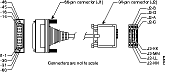
Figure C-4 shows the V.35 serial cable assembly. Table C-6 lists the DTE pinouts, and Table C-7 lists the DCE pinouts. Arrows indicate signal direction: --> indicates DTE to DCE, and <-- indicates DCE to DTE.
| 60 Pin | Signal Name | Type | Direction | 34 Pin | Signal Name |
|---|---|---|---|---|---|
| J1-49 J1-48 | MODE_1 GND | Shorting group | - | - | - |
| J1-50 J1-51 J1-52 | MODE_0 GND MODE_DCE | Shorting group | - | - | - |
| J1-53 J1-54 J1-55 J1-56 | TxC/NIL RxC_TxCE RxD/TxD GND | Shorting group | - | - | - |
| J1-46 | Shield_GND | Single | - | J2-A | Frame GND |
| J1-45 Shield | Circuit_GND - | Twisted pair no. 12 | - - | J2-B Shield | Circuit GND - |
| J1-42 Shield | RTS/CTS - | Twisted pair no. 9 | --> - | J2-C Shield | RTS - |
| J1-35 Shield | CTS/RTS - | Twisted pair no. 8 | <-- - | J2-D Shield | CTS - |
| J1-34 Shield | DSR/DTR - | Twisted pair no. 7 | <-- - | J2-E Shield | DSR - |
| J1-33 Shield | DCD/LL - | Twisted pair no. 6 | <-- - | J2-F Shield | RLSD - |
| J1-43 Shield | DTR/DSR - | Twisted pair no. 10 | --> - | J2-H Shield | DTR - |
| J1-44 Shield | LL/DCD - | Twisted pair no. 11 | --> - | J2-K Shield | LT - |
| J1-18 J1-17 | TxD/RxD+ TxD/RxD- | Twisted pair no. 1 | --> --> | J2-P J2-S | SD+ SD- |
| J1-28 J1-27 | RxD/TxD+ RxD/TxD- | Twisted pair no. 5 | <-- <-- | J2-R J2-T | RD+ RD- |
| J1-20 J1-19 | TxCE/TxC+ TxCE/TxC- | Twisted pair no. 2 | --> --> | J2-U J2-W | SCTE+ SCTE- |
| J1-26 J1-25 | RxC/TxCE+ RxC/TxCE- | Twisted pair no. 4 | <-- <-- | J2-V J2-X | SCR+ SCR- |
| J1-24 J1-23 | TxC/RxC+ TxC/RxC- | Twisted pair no. 3 | <-- <-- | J2-Y J2-AA | SCT+ SCT- |
| 60 Pin | Signal Name | Type | Direction | 34 Pin | Signal Name |
|---|---|---|---|---|---|
| J1-49 J1-48 | MODE_1 GND | Shorting group | - | - | - |
| J1-50 J1-51 | MODE_0 GND | Shorting group | - | - | - |
| J1-53 J1-54 J1-55 J1-56 | TxC/NIL RxC_TxCE RxD/TxD GND | Shorting group | - | - | - |
| J1-46 | Shield_GND | Single | - | J2-A | Frame GND |
| J1-45 Shield | Circuit_GND - | Twisted pair no. 12 | - - | J2-B Shield | Circuit GND - |
| J1-35 Shield | CTS/RTS - | Twisted pair no. 8 | <-- - | J2-C Shield | RTS - |
| J1-42 Shield | RTS/CTS - | Twisted pair no. 9 | --> - | J2-D Shield | CTS - |
| J1-43 Shield | DTR/DSR - | Twisted pair no. 10 | --> - | J2-E Shield | DSR - |
| J1-44 Shield | LL/DCD - | Twisted pair no. 11 | --> - | J2-F Shield | RLSD - |
| J1-34 Shield | DSR/DTR - | Twisted pair no. 7 | <-- - | J2-H Shield | DTR - |
| J1-33 Shield | DCD/LL - | Twisted pair no. 6 | <-- - | J2-K Shield | LT - |
| J1-28 J1-27 | RxD/TxD+ RxD/TxD- | Twisted pair no. 5 | <-- <-- | J2-P J2-S | SD+ SD- |
| J1-18 J1-17 | TxD/RxD+ TxD/RxD- | Twisted pair no. 1 | --> --> | J2-R J2-T | RD+ RD- |
| J1-26 J1-25 | RxC/TxCE+ RxC/TxCE- | Twisted pair no. 4 | <-- <-- | J2-U J2-W | SCTE+ SCTE- |
| J1-22 J1-21 | NIL/RxC+ NIL/RxC- | Twisted pair no. 3 | --> --> | J2-V J2-X | SCR+ SCR- |
| J1-20 J1-19 | TxCE/TxC+ TxCE/TxC- | Twisted pair no. 2 | --> --> | J2-Y J2-AA | SCT+ SCT- |
Figure C-5 shows the X.21 serial cable assembly. Table C-8 lists the DTE pinouts, and Table C-9 lists the DCE pinouts. Arrows indicate signal direction: --> indicates DTE to DCE, and <-- indicates DCE to DTE.
| 60 Pin | Signal Name | Type | Direction | 15 Pin | Signal Name |
|---|---|---|---|---|---|
| J1-48 J1-47 | GND MODE_2 | Shorting group | - | - | - |
| J1-51 J1-52 | GND MODE_DCE | Shorting group | - | - | - |
| J1-46 | Shield_GND | Single | - | J2-1 | Shield GND |
| J1-11 J1-12 | TXD/RXD+ TXD/RXD- | Twisted pair no. 3 | --> --> | J2-2 J2-9 | Transmit+ Transmit- |
| J1-9 J1-10 | RTS/CTS+ RTS/CTS- | Twisted pair no. 2 | --> --> | J2-3 J2-10 | Control+ Control- |
| J1-28 J1-27 | RXD/TXD+ RXD/TXD- | Twisted pair no. 6 | <-- <-- | J2-4 J2-11 | Receive+ Receive- |
| J1-1 J1-2 | CTS/RTS+ CTS/RTS- | Twisted pair no. 1 | <-- <-- | J2-5 J2-12 | Indication+ Indication- |
| J1-26 J1-25 | RXC/TXCE+ RXC/TXCE- | Twisted pair no. 5 | <-- <-- | J2-6 J2-13 | Timing+ Timing- |
| J1-15 Shield | Control_GND - | Twisted pair no. 4 | - - | J2-8 Shield | Control GND - |
| 60 Pin | Signal Name | Type | Direction | 15 Pin | Signal Name |
|---|---|---|---|---|---|
| J1-48 J1-47 | GND MODE_2 | Shorting group | - | - | - |
| J1-46 | Shield_GND | Single | - | J2-1 | Shield GND |
| J1-28 J1-27 | RXD/TXD+ RXD/TXD- | Twisted pair no. 6 | <-- <-- | J2-2 J2-9 | Transmit+ Transmit- |
| J1-1 J1-2 | CTS/RTS+ CTS/RTS- | Twisted pair no. 1 | <-- <-- | J2-3 J2-10 | Control+ Control- |
| J1-11 J1-12 | TXD/RXD+ TXD/RXD- | Twisted pair no. 3 | --> --> | J2-4 J2-11 | Receive+ Receive- |
| J1-9 J1-10 | RTS/CTS+ RTS/CTS- | Twisted pair no. 2 | --> --> | J2-5 J2-12 | Indication+ Indication- |
| J1-24 J1-23 | TXC/RXC+ TXC/RXC- | Twisted pair no. 4 | --> --> | J2-6 J2-13 | Timing+ Timing- |
| J1-15 Shield | Control_GND - | Twisted pair no. 5 | - - | J2-8 Shield | Control GND - |
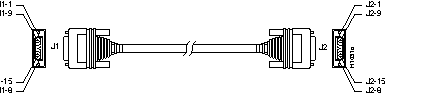
Figure C-6 shows the EIA-530 serial cable assembly, and Table C-10 lists the pinouts. Arrows indicate signal direction: --> indicates DTE to DCE, and <-- indicates DCE to DTE.
60 Pin | Signal Name | 25 Pin | Signal Name | Direction DTE DCE1 |
|---|---|---|---|---|
| J1-11 J1-12 | TXD/RXD+ TXD/RXD- | J2-2 J2-14 | BA(A), TXD+ BA(B), TXD- | --> --> |
| J1-28 J1-27 | RXD/TXD+ RXD/TXD- | J2-3 J2-16 | BB(A), RXD+ BB(B), RXD- | <-- <-- |
| J1-9 J1-10 | RTS/CTS+ RTS/CTS- | J2-4 J2-19 | CA(A), RTS+ CA(B), RTS- | --> --> |
| J1-1 J1-2 | CTS/RTS+ CTS/RTS- | J2-5 J2-13 | CB(A), CTS+ CB(B), CTS- | <-- <-- |
| J1-3 J1-4 | DSR/DTR+ DSR/DTR- | J2-6 J2-22 | CC(A), DSR+ CC(B), DSR- | <-- <-- |
| J1-46 J1-47 | Shield_GND MODE_2 | J2-1 - | Shield - | Shorted |
| J1-48 J1-49 | GND MODE_1 | - - | - - | Shorted |
| J1-5 J1-6 | DCD/DCD+ DCD/DCD- | J2-8 J2-10 | CF(A), DCD+ CF(B), DCD- | <-- <-- |
| J1-24 J1-23 | TXC/RXC+ TXC/RXC- | J2-15 J2-12 | DB(A), TXC+ DB(B), TXC- | <-- <-- |
| J1-26 J1-25 | RXC/TXCE+ RXC/TXCE- | J2-17 J2-9 | DD(A), RXC+ DD(B), RXC- | <-- <-- |
| J1-44 J1-45 | LL/DCD Circuit_GND | J2-18 J2-7 | LL Circuit_ GND | --> - |
| J1-7 J1-8 | DTR/DSR+ DTR/DSR- | J2-20 J2-23 | CD(A), DTR+ CD(B), DTR- | --> --> |
| J1-13 J1-14 | TXCE/TXC+ TXCE/TXC- | J2-24 J2-11 | DA(A), TXCE+ DA(B), TXCE- | --> --> |
| J1-51 J1-52 | GND MODE_DCE | - - | - - | Shorted |
Use a UTP, STP, or fiber-optic cable to connect the MII port on a 1-port Fast Ethernet network module to a 100BaseTX, 100BaseFX, or 100BaseT4 transceiver. (See Figure 1.) The type of cable you need depends on the transceiver.
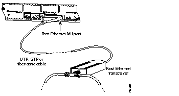
? This illustration is a modification of an older one, and it looks like the transceiver needs some work. What does a Fast Ethernet transceiver look like?
The module detects the type of network connection automatically, and you do not need to select the media type in software. If cables are plugged into both the 100BaseTX connector and the MII connector, the 100BaseTX connection is selected.
Figure C-1 shows the 100BaseTX RJ-45 connector, and Table C-1 lists its pinout. The 1-port Fast Ethernet network module RJ-45 port actively terminates wire pair 4 and 5 and wire pair 7 and 8. Common-mode termination reduces electromagnetic interference (EMI) and susceptibility to common-mode sources.
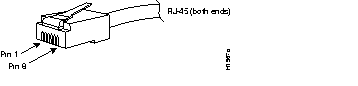
| Pin | Signal |
|---|---|
| 1 | TX+ |
| 2 | TX- |
| 3 | RX+ |
| 6 | RX- |
The following figures and tables provide the pinouts and signal descriptions for the Ethernet AUI cable and 10BaseT connector.
Figure C-2 shows the Ethernet AUI cable assembly and Table C-2 lists the pinouts.
| Pin1 | Ethernet Circuit | Signal Name |
|---|---|---|
| 3 | DO-A | Data Out Circuit A |
| 10 | DO-B | Data Out Circuit B |
| 11 | DO-S | Data Out Circuit Shield |
| 5 | DI-A | Data In Circuit A |
| 12 | DI-B | Data In Circuit B |
| 4 | DI-S | Data In Circuit Shield |
| 7 | CO-A | Control Out Circuit A (not connected) |
| 15 | CO-B | Control Out Circuit B (not connected) |
| 8 | CO-S | Control Out Circuit Shield (not connected) |
| 2 | CI-A | Control In Circuit A |
| 9 | CI-B | Control In Circuit B |
| 1 | CI-S | Control In Circuit Shield |
| 6 | VC | Voltage Common |
| 13 | VP | Voltage Plus |
| 14 | VS | Voltage Shield (L25 and M25) |
| Shell | PG | Protective Ground |
Figure C-3 shows the 10BaseT connector (RJ-45) and Table C-3 lists the pinouts.

| Pin1 | Description |
|---|---|
| 1 | TX+ |
| 2 | TX- |
| 3 | RX+ |
| 4 | - |
| 5 | - |
| 6 | RX- |
| 7 | - |
| 8 | - |
The 1E1R 2-slot module provides both UTP and STP Token Ring connections.
Table C-4 shows the Token Ring STP port pinouts used by the 1E1R 2-slot module.
| 9-Pin | Signal Name |
|---|---|
| 1 | RX- |
| 2 | Ground |
| 3 | +5 Volt, fused |
| 4 | Ground |
| 5 | TX- |
| 6 | RX+ |
| 7 | Ground |
| 8 | Ground |
| 9 | TX+ |
Table C-5 shows the Token Ring UTP port pinouts used by the 1E1R 2-slot module.
| RJ-45 Pins | Signal |
|---|---|
| 1 | GND |
| 2 | GND |
| 3 | TX |
| 4 | RX |
| 5 | TX |
| 6 | RX |
| 7 | GND |
| 8 | Not used |
The BRI interface port pinouts are listed in Table C-6.
| 8 Pin1 | TE2 | NT3 | Polarity |
|---|---|---|---|
| 3 | Transmit | Receive | + |
| 4 | Receive | Transmit | + |
| 5 | Receive | Transmit | - |
| 6 | Transmit | Receive | - |
 | Caution To prevent damage to the system, make certain you connect the BRI cable to the BRI connector only and not to any other RJ-45 connector. |
Two standard T1 serial cables are available for the CT1/PRI module: straight-through and null-modem. A straight-through cable connects the router to an external CSU. Null-modem cables are used for back-to-back operation and testing.
The T1 interface cable has two 15-pin DB connectors at each end to connect the CT1/PRI module with the external T1 CSU. Figure C-4 shows the T1 interface cable, connectors, and pinouts. Table C-7 lists the pinouts for the null-modem T1 cable, and Table C-8 lists the pinouts for the straight-through T1 cable.
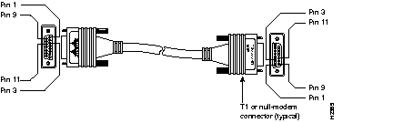
| 15-Pin DB Connector | 15-Pin DB Connector | ||
|---|---|---|---|
| Signal | Pin | Pin | Signal |
| Transmit Tip | 1 | 3 | Receive Tip |
| Receive Tip | 3 | 1 | Transmit Tip |
| Transmit Ring | 9 | 11 | Receive Ring |
| Receive Ring | 11 | 9 | Transmit Ring |
| 15-Pin DB Connector | 15-Pin DB Connector | ||
|---|---|---|---|
| Signal | Pin | Pin | Signal |
| Transmit Tip | 1 | 1 | Transmit Tip |
| Transmit Ring | 9 | 9 | Transmit Ring |
| Receive Tip | 3 | 3 | Receive Tip |
| Receive Ring | 11 | 11 | Receive Ring |
Table C-9 lists the CT1/PRI-CSU module port pinouts. Use a straight-through RJ-48C-to-RJ-48C cable to connect the T1 port to an RJ-48C jack.
| RJ-48C Pin | Description |
|---|---|
| 1 | Receive Ring |
| 2 | Receive Tip |
| 4 | Ring |
| 5 | Tip |
There are three serial cables for the 120-ohm CE1/PRI-B modules and one serial cable for the 75-ohm CE1/PRI-U modules. All four E1 cables have DB-15 connectors on the router end. The cables for the CE1/PRI-B modules have either DB-15, Twinax, or RJ-45 connectors on the network end. The cable for the CE1/PRI-U modules have a BNC connector at the network end. Figure C-5 to Figure C-8 show the CE1/PRI cables.


Table C-10 lists the pinouts for the CE1/PRI module cable pinouts.
| CE1/PRI End | Network End | |||||||
|---|---|---|---|---|---|---|---|---|
| DB-15 | BNC | DB-15 | Twinax | RJ-45 | ||||
| Pin | Signal | Signal | Pin | Signal | Pin | Signal | Pin | Signal |
| 9 | Tx Tip | Tx Tip | 1 | Tx Tip | Tx-1 | Tx Tip | 1 | Tx Tip |
| 2 | Tx Ring | Tx Shield | 9 | Tx Ring | Tx-2 | Tx Ring | 2 | Tx Ring |
| 10 | Tx Shield | - | 2 | Tx Shield | Shield | Tx Shield | 3 | Tx Shield |
| 8 | Rx Tip | Rx Tip | 3 | Rx Tip | Rx-1 | Rx Tip | 4 | Rx Tip |
| 15 | Rx Ring | Rx Shield | 11 | Rx Ring | Rx-2 | Rx Ring | 5 | Rx Ring |
| 7 | Rx Shield | - | 4 | Rx Shield | Shield | Rx Shield | 6 | Rx Shield |
The 1-port 4-wire 56 kbps DSU/CSU WAN interface card uses a straight-through RJ-48S-to-RJ-48S cable. Table C-11 provides pinouts.
| RJ-48S Pins1 | Signal |
|---|---|
| 1 | Receive Ring |
| 2 | Receive Tip |
| 7 | Ring |
| 8 | Tip |
|
|