|
|

This chapter contains information about troubleshooting, enabling booting from Flash memory, copying to Flash memory, and cable pinouts. For additional information about the Cisco 2500 series router hardware, refer to the Cisco 2500 Series Hardware Installation and Maintenance publication.
The key to problem solving in this system is to try to isolate the problem to a specific subsystem. By comparing what the system is doing to what it should be doing, the task of isolating a problem is greatly simplified.
Troubleshooting might require copying or reloading the operating system image from Flash memory or testing cables. Flash memory and cable information is included in this chapter.
Check the following items to help isolate the problem:
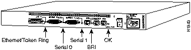
The green OK LED (to the right of the AUX port) should be ON after the system initializes correctly. (See Figure 3-1.)
Figure 3-1 Router LEDs---Rear-Panel View
For more complete network troubleshooting information, refer to the Troubleshooting Internetworking Systems publication.
To enable booting from Flash memory, set configuration register bits 3, 2, 1, and 0 to a value between 2 and 15 in conjunction with the boot system flash [filename] configuration command.
To enter the configuration mode, while in the system software image specify a Flash filename from which to boot, enter the configure terminal command at the enable prompt, as in the example following:
router# configure terminal
Enter configuration commands, one per line.
Edit with DELETE, CTRL/W, and CTRL/U; end with CTRL/Z
boot system flash [filename]
To disable break and enable the boot system flash command, enter the config-register command with the value shown in the example following:
router# config term
Enter configuration commands, one per line.
Edit with DELETE, CTRL/W, and CTRL/U; end with CTRL/Z
config-reg 0x2102
^Z
router#
Copying a new image to Flash memory might be required whenever a new image or maintenance release becomes available. To copy a new image into Flash memory (write to Flash memory), you must first reboot from ROM and then copy the new image into Flash memory. You cannot copy a new image into Flash memory while the system is running from Flash memory. Use the copy tftp flash command for the copy procedure.
Following is a sample output for setting the configuration register to 0x2101, which tells the system to boot from ROM, but does not reset the break disable or check for a default netboot filename.
router# configure terminal
Enter configuration commands, one per line.
  Edit with DELETE, CTRL/W, and CTRL/U; end with CTRL/Z
config-reg 0x2101
^Z
Following is sample output for reloading the router and then copying a file (called IJ09140Z) to Flash memory from a TFTP server (called server1):
router# reload
...
router(boot)# copy tftp flash
File  Length   Name/status
  1   4035664     IJ09140Y
[4035728 bytes used, 158576 available, 4194304 total]
Address or name of remote host [255.255.255.255]? server1
Source file name? IJ09140Z
Destination file name [default = source name]? <Return>
Accessing file 'IJ09140Z' on 131.108.1.111...
Loading IJ09140Z from 131.108.1.111 (via Ethernet0): !
Erase flash device before writing? [confirm]y
Flash contains files. Are you sure? [confirm]y
Copy 'IJ09140Z' from TFTP server
as 'IJ09140Z' into Flash WITH erase? [yes/no] y
Erasing device...  ... erased
Loading IJ09140Z from 131.108.1.111 (via Ethernet0):
!!!!!!!!!!!!!!!!!!!!!!!!!!!!!!!!!!!!!!!!!!!!!!!!!!!!!!!!!!!!!!!!!!!!!!!!
!!!!!!!!!!!!!!!!!!!!!!!!!!!!!!!!!!!!!!!!!!!!!!!!!!!!!!!!!!!!!!!!!!!!!!!!
!!!!!!!!!!!!!!!!!!!!!!!!!!!!!!!!!!!!!!!!!!!!!!!!!!!!!!!!!!!!!!!!!!!!!!!!
!!!!!!!!!!!!!!!!!!!!!!!!!!!!!!!!!!!!!!!!!!!!!!!!!!!!!!!!!!!!!!!!!!!.!!.!
!!!!!!!!!!!!!!!!!!!!!!!!.!!!!!!!!!!!!!!!!!!!!!!!!!!!!!!!!!!!!!!!!!!!!!!!
!!!!!!!!!!!!!!!!!!!!!!!!!!!!!!!!!.!!!!!!!!!!!!!!!!!!!!!!!.!!!!!!!!!!!!!!
!!!!!!!!!!!!!!!!!!!!!!!!!!!!!!!!!!!!!!!!!!!!!!!!!!!!!!!!!!!!!!!!!!!!!!!!
!!!!!!!!!!!!!!!!!!!!!!!!!!!!!!!!!!!!!!!!!!!!!!!!!!!!!!!!!!!!!!!!!!!!!!!!
!!!!!!!!!!!!!!!!!!!!!!!!!!!!!!!!!!!!!!!!!!!!!!!!!!!!!!!!!!!!!
[OK - 3235932/8 388608 bytes]
Verifying checksum...  OK (0x6871)
Flash copy took 60700 msecs
Following is a sample output for setting the configuration register to 0x2102, which tells the system to boot from ROM if netboot fails, disable break, and check for a default netboot filename.
router(boot)#         config term
Enter configuration commands, one per line.
Edit with DELETE, CTRL/W, and CTRL/U; end with CTRL/Z
config-reg 0x2102
^Z
After copying the file (called IJ09140Z) to Flash memory from a TFTP server (called server1), the router is reloaded, as follows:
router(boot)# reload
...
The system is now ready to be configured to boot from the new image you copied to Flash memory. For more information on the copy tftp flash command, and other related commands, refer to the router products configuration publication
The following tables list the pinouts for the cables that can be used with the 2500 series products:
Table 3-1 Console Port Pinouts (RJ-45)
| Pin(1) | Signal | Input/Output |
|---|---|---|
| 1 | -- | -- |
| 2 | DTR | Output |
| 3 | TXD | Output |
| 4 | GND | -- |
| 5 | GND | -- |
| 6 | RXD | Input |
| 7 | CD | Input |
| 8 | -- | -- |
Table 3-2 Auxiliary Port Pinouts (RJ-45)
| Pin(1) | Signal | Input/Output |
|---|---|---|
| 1 | RTS | Output |
| 2 | DTR | Output |
| 3 | TXD | Output |
| 4 | GND | -- |
| 5 | GND | -- |
| 6 | RXD | Input |
| 7 | CD | Input |
| 8 | CTS | Input |
The connection of pins between the RJ-45 connector and the end device depends on the type of cable and adapter used. Either a straight or rolled cable can be used. Refer to Table 3-3 for the pinout of a straight and a rolled cable. The Cisco 2500 series products now ship with a rolled cable. Refer to Table 3-4 for a list of the pins used on the RJ-45 connector, the male/female DTE (MDTE/FDTE) adapter, the male/female DCE (MDTE/FDTE) adapter, and the male modem (MMOD) adapter used to connect terminals and modems to Cisco 2500 series products. Refer to Table 3-5 for the cable and adapter configurations that can be used to connect terminals and modems to Cisco 2500 series products.
Table 3-3 RJ-45 Straight and Rolled Cables
| RJ-45 Pins | Straight Cable Pinout |
Rolled Cable Pinout |
|---|---|---|
| 1 | 1 | 8 |
| 2 | 2 | 7 |
| 3 | 3 | 6 |
| 4 | 4 | 5 |
| 5 | 5 | 4 |
| 6 | 6 | 3 |
| 7 | 7 | 2 |
| 8 | 8 | 1 |
Table 3-4 Pins for the RJ-45, MDTE/FDTE, MDCE/FDCE, and MMOD
| Cable | DB-25 Adapters | ||
|---|---|---|---|
| RJ-45 Pins | MDTE/FDTE Pins(1) | MDCE/MDTE Pins | MMOD Pins(2) |
| 1 | 4 | 5 | 5 |
| 2 | 20 | 6 | 8 |
| 3 | 2 | 3 | 3 |
| 4 | 7 | 7 | 7 |
| 5 | 7 | 7 | 7 |
| 6 | 3 | 2 | 2 |
| 7 | 6 | 20 | 20 |
| 8 | 5 | 4 | 4 |
Table 3-5 Connection Configuration
| Cisco 2500 Port | RJ-45 Cable Type | DB-25 Adapter | End Device |
|---|---|---|---|
| Console | Rolled | MDTE/FDTE | Terminal |
| Console | Straight | MDCE/FDCE | Terminal |
| Console(1) | Rolled | MMOD | Modem |
| Aux | Rolled | MDTE/FDTE | Terminal |
| Aux | Straight | MDCE/FDCE | Terminal |
| Aux | Rolled | MMOD | Modem |
Figure 3-2 RJ-45-to-DB-9 Adapter Pinouts
| RJ-45 Pin | Signal | DB-9 Pin |
|---|---|---|
| 1 | RTS | 7 |
| 2 | DTR | 4 |
| 3 | TXD | 3 |
| 4 | GND | 5 |
| 5 | GND | 5 |
| 6 | RXD | 2 |
| 7 | DSR | 6 |
| 8 | CTS | 8 |
Table 3-6 BRI Port Pinout (RJ-45)
| 8 Pin(1) | TE(2) | NT(3) | Polarity |
|---|---|---|---|
| 3 | Transmit | Receive | + |
| 4 | Receive | Transmit | + |
| 5 | Receive | Transmit | -- |
| 6 | Transmit | Receive | -- |
![]()
Table 3-7 EIA-530 DTE Serial Cable Pinout (DB-25)
| 25 Pin(1) | Signal | DirectionDTE DCE(2) | 25 Pin | Signal | DirectionDTE DCE |
|---|---|---|---|---|---|
| J2-1-- | Shield-- | ---- | J2-8J2-10 | CF(A), DCD+CF(B), DCD-- | <---<--- |
| J2-2J2-14 | BA(A), TxD+BA(B), TxD-- | --->---> | J2-15J2-12 | DB(A), TxC+DB(B), TxC-- | <---<--- |
| J2-3J2-16 | BB(A), RxD+BB(B), RxD-- | <---<--- | J2-17J2-9 | DD(A), RxC+DD(B), RxC-- | <---<--- |
| J2-4J2-19 | CA(A), RTS+CA(B), RTS-- | --->---> | J2-18J2-7 | LL Circuit GND | --->-- |
| J2-5J2-13 | CB(A), CTS+ CB(B), CTS-- | <---<--- | J2-20J2-23 | CD(A), DTR+CD(B), DTR-- | --->---> |
| J2-6J2-22 | CC(A), DSR+ CC(B), DSR-- | <---<--- | J2-24J2-11 | DA(A), TxCE+DA(B), TxCE-- | --->---> |
Table 3-8 EIA/TIA-232 DTE and DCE Serial Cable Pinouts (DB-25)
| 25 Pin(1) | Signal | DirectionDTE DCE | 25 Pin | Signal | DirectionDTE DCE |
|---|---|---|---|---|---|
| J2-1 | Shield GND | _ | J2-7Shield | Circuit GND-- | ---- |
| J2-2Shield | TxD-- | --->-- | J2-8Shield | DCD-- | <----- |
| J2-3Shield | RxD-- | <----- | J2-15Shield | TxC-- | <----- |
| J2-4Shield | RTS-- | --->-- | J2-17Shield | RxC -- | <----- |
| J2-5Shield | CTS-- | <----- | J2-18Shield | LTST-- | --->-- |
| J2-6Shield | DSR-- | <----- | J2-20Shield | DTR-- | --->-- |
| J2-24Shield | TxCE-- | --->-- |
Table 3-9 EIA/TIA-449 DTE and DCE Serial Cable Pinouts (DB-37)
| 37 Pin(1) | Signal | DirectionDTE DCE | 37 Pin | Signal | DirectionDTE DCE |
|---|---|---|---|---|---|
| J2-1 | Shield GND | -- | J2-9J2-27 | CS+CS-- | --->---> |
| J2-4J2-22 | SD+SD-- | <---<--- | J2-10J2-37 | LLSC | --->-- |
| J2-5J2-23 | ST+ST-- | --->---> | J2-11J2-29 | DM+DM-- | --->---> |
| J2-6J2-24 | RD+RD-- | --->---> | J2-12J2-30 | TR+TR-- | <---<--- |
| J2-7J2-25 | RS+RS-- | <---<--- | J2-13J2-31 | RR+RR-- | --->---> |
| J2-8J2-26 | RT+RT-- | --->---> | J2-17J2-35 | TT+TT-- | <---<--- |
| J2-19J2-20 | SGRC | ---- |
Table 3-10 V.35 DTE and DCE Serial Cable Pinouts (Winchester-Type 34 Pin)
| 34 Pin(1) | Signal | DirectionDTE DCE | 34 Pin | Signal | DirectionDTE DCE |
|---|---|---|---|---|---|
| J2-A | Frame GND | -- | J2-HShield | DTR-- | --->-- |
| J2-BShield | Circuit GND-- | ---- | J2-KShield | LT-- | --->-- |
| J2-CShield | RTS-- | --->-- | J2-PJ2-S | SD+SD-- | --->---> |
| J2-DShield | CTS-- | <----- | J2-RJ2-T | RD+RD-- | <---<--- |
| J2-EShield | DSR-- | <----- | J2-UJ2-W | SCTE+SCTE-- | --->---> |
| J2-FShield | RLSD-- | <----- | J2-VJ2-X | SCR+SCR-- | <---<--- |
| J2-YJ2-AA | SCT+SCT-- | <---<--- |
Table 3-11 X.21 DTE and DCE Serial Cable Pinouts (DB-15)
| 15 Pin(1) | Signal | DirectionDTE DCE |
|---|---|---|
| J2-1 | Shield GND | -- |
| J2-2J2-9 | Transmit+Transmit-- | --->---> |
| J2-3J2-10 | Control+Control-- | --->---> |
| J2-4J2-11 | Receive+Receive-- | <---<--- |
| J2-5J2-12 | Indication+Indication-- | <---<--- |
| J2-6J2-13 | Timing+Timing-- | <---<--- |
| J2-8Shield | Circuit GND-- | ---- |
Table 3-12 Ethernet (AUI) Port Pinout (DB-15)
| 15 Pin | Ethernet Circuit | Signal |
|---|---|---|
| 1 | CI-S | Control In Circuit Shield |
| 2 | CI-A | Control In Circuit A |
| 3 | DO-A | Data Out Circuit A |
| 4 | DI-S | Data In Circuit Shield |
| 5 | DI-A | Data In Circuit A |
| 6 | VC | Voltage Common |
| 7 | CO-A | Control Out Circuit A (not connected) |
| 8 | CO-S | Control Out Circuit Shield (not connected) |
| 9 | CI-B | Control In Circuit B |
| 10 | DO-B | Data Out Circuit B |
| 11 | DO-S | Data Out Circuit Shield |
| 12 | DI-B | Data In Circuit B |
| 13 | VP | Voltage Plus |
| 14 | VS | Voltage Shield (L25 and M25) |
| 15 | CO-B | Control Out Circuit B (not connected) |
| Shell | PG | Protective Ground |
Table 3-13 Ethernet 10BaseT Port Pinout (RJ-45)
| Pin | Signal |
|---|---|
| 1 | TX+ |
| 2 | TX-- |
| 3 | RX+ |
| 4 | -- |
| 5 | -- |
| 6 | RX-- |
| 7 | -- |
| 8 | -- |
Table 3-14 Token Ring Port Pinout (DB-9)
| 9 Pin(1) | Signal |
|---|---|
| 1 | Receive R1-- |
| 3 | +5V(2) |
| 5 | Transmit O5-- |
| 6 | Receive G6+ |
| 9 | Transmit B9+ |
Table 3-15 Asynchronous Breakout Cable Pinout (8-Pin RJ-45)
| 8-Pin RJ-45 | Signal | Direction |
|---|---|---|
| 1 | CTS | <--- |
| 2 | DSR/DCD | <--- |
| 3 | RXD | <--- |
| 4 | RXD/GND | - |
| 5 | TXD/GND | - |
| 6 | TXD | ---> |
| 7 | DTR | ---> |
| 8 | RTS | ---> |
Table 3-16 Asynchronous-Line Cable Pinout (68-Pin SCSI)
| RJ-45 Plug | Pin | Signal | 68-Pin SCSI (J1) |
|---|---|---|---|
| 1 | 8 | RTS | 2 |
| 7 | DTR | 36 | |
| 6 | TXD | 3 | |
| 5 | TXD GND | 37 | |
| 4 | RXD GND | 4 | |
| 3 | RXD | 38 | |
| 2 | DSR | 5 | |
| 1 | CTS | 39 | |
| 2 | 8 | RTS | 6 |
| 7 | DTR | 40 | |
| 6 | TXD | 7 | |
| 5 | TXD GND | 41 | |
| 4 | RXD GND | 8 | |
| 3 | RXD | 42 | |
| 2 | DSR | 9 | |
| 1 | CTS | 43 | |
| 3 | 8 | RTS | 10 |
| 7 | DTR | 44 | |
| 6 | TXD | 11 | |
| 5 | TXD GND | 45 | |
| 4 | RXD GND | 12 | |
| 3 | RXD | 46 | |
| 2 | DSR | 13 | |
| 1 | CTS | 47 | |
| 4 | 8 | RTS | 14 |
| 7 | DTR | 48 | |
| 6 | TXD | 15 | |
| 5 | TXD GND | 49 | |
| 4 | RXD GND | 16 | |
| 3 | RXD | 50 | |
| 2 | DSR | 17 | |
| 1 | CTS | 51 | |
| 5 | 8 | RTS | 18 |
| 7 | DTR | 52 | |
| 6 | TXD | 19 | |
| 5 | TXD GND | 53 | |
| 4 | RXD GND | 20 | |
| 3 | RXD | 54 | |
| 2 | DSR | 21 | |
| 1 | CTS | 55 | |
| 6 | 8 | RTS | 22 |
| 7 | DTR | 56 | |
| 6 | TXD | 23 | |
| 5 | TXD GND | 57 | |
| 4 | RXD GND | 24 | |
| 3 | RXD | 58 | |
| 2 | DSR | 25 | |
| 1 | CTS | 59 | |
| 7 | 8 | RTS | 26 |
| 7 | DTR | 60 | |
| 6 | TXD | 27 | |
| 5 | TXD GND | 61 | |
| 4 | RXD GND | 28 | |
| 3 | RXD | 62 | |
| 2 | DSR | 29 | |
| 1 | CTS | 63 | |
| 8 | 8 | RTS | 30 |
| 7 | DTR | 64 | |
| 6 | TXD | 31 | |
| 5 | TXD GND | 65 | |
| 4 | RXD GND | 32 | |
| 3 | RXD | 66 | |
| 2 | DSR | 33 | |
| 1 | CTS | 67 |
Figure 3-3 shows the DB-25 breakout cable with pinouts for the 68-pin SCSI port and the DB-25 port. Table 3-17 lists the pinouts for the DB-25 end, and Table 3-18 lists the pinouts for the 68-pin SCSI connector end.
Figure 3-3 Asynchronous Serial Interface Breakout Cable Assembly (68-Pin SCSI-to-DB-25)
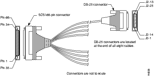
Table 3-17 Asynchronous Breakout Cable Pinouts (DB-25)
| DB-25 Plug(1) | Signal | Direction |
|---|---|---|
| 4 | RTS | ---> |
| 20 | DTR | ---> |
| 2 | TXD | ---> |
| 7 | TXD GND | --- |
| 7 | RXD GND | --- |
| 3 | RXD | <--- |
| 8 | DSR | <--- |
| 5 | CTS | <--- |
Table 3-18 Asynchronous Cable Pinouts (68-Pin SCSI-to-DB-25)
| DB-25 Plug | Pin | Signal | 68-Pin SCSI (J1) |
|---|---|---|---|
| 1 | 4 | RTS | 2 |
| 20 | DTR | 36 | |
| 2 | TXD | 3 | |
| 7 | TXD GND | 37 | |
| 7 | RXD GND | 4 | |
| 3 | RXD | 38 | |
| 8 | DSR | 5 | |
| 5 | CTS | 39 | |
| 2 | 4 | RTS | 6 |
| 20 | DTR | 40 | |
| 2 | TXD | 7 | |
| 7 | TXD GND | 41 | |
| 7 | RXD GND | 8 | |
| 3 | RXD | 42 | |
| 8 | DSR | 9 | |
| 5 | CTS | 43 | |
| 3 | 4 | RTS | 10 |
| 20 | DTR | 44 | |
| 2 | TXD | 11 | |
| 7 | TXD GND | 45 | |
| 7 | RXD GND | 12 | |
| 3 | RXD | 46 | |
| 8 | DSR | 13 | |
| 5 | CTS | 47 | |
| 4 | 4 | RTS | 14 |
| 20 | DTR | 48 | |
| 2 | TXD | 15 | |
| 7 | TXD GND | 49 | |
| 7 | RXD GND | 16 | |
| 3 | RXD | 50 | |
| 8 | DSR | 17 | |
| 5 | CTS | 51 | |
| 5 | 4 | RTS | 18 |
| 20 | DTR | 52 | |
| 2 | TXD | 19 | |
| 7 | TXD GND | 53 | |
| 7 | RXD GND | 20 | |
| 3 | RXD | 54 | |
| 8 | DSR | 21 | |
| 5 | CTS | 55 | |
| 6 | 4 | RTS | 22 |
| 20 | DTR | 56 | |
| 2 | TXD | 23 | |
| 7 | TXD GND | 57 | |
| 7 | RXD GND | 24 | |
| 3 | RXD | 58 | |
| 8 | DSR | 25 | |
| 5 | CTS | 59 | |
| 7 | 4 | RTS | 26 |
| 20 | DTR | 60 | |
| 2 | TXD | 27 | |
| 7 | TXD GND | 61 | |
| 7 | RXD GND | 28 | |
| 3 | RXD | 62 | |
| 8 | DSR | 29 | |
| 5 | CTS | 63 | |
| 8 | 4 | RTS | 30 |
| 20 | DTR | 64 | |
| 2 | TXD | 31 | |
| 7 | TXD GND | 65 | |
| 7 | RXD GND | 32 | |
| 3 | RXD | 66 | |
| 8 | DSR | 33 | |
| 5 | CTS | 67 |
|
|
Copyright 1988-1995 © Cisco Systems Inc.