|
|

The Channelized Data PAD (CDP) is a dual-purpose front card that provides a method of terminating a T1, E1, or J1 circuit line.
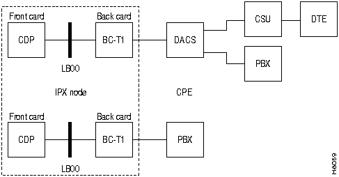
The CDP interfaces to lines that can carry voice traffic, a combination of voice and low-speed and high-speed data circuits, or just data. For examples of CDP configuration in a system, see Figure 1-28. The CDP data capabilities include DS0-A, 56/64 x n data rates. The CDP voice capabilities include A-law to m-Law per-channel conversion and high per-channel voice compression levels.
A CDP can go in any front slot not reserved for a processor card. The CDP works with a BC-T1, BC-E1, or BC-J1 back card in the associated rear slot.
Figure 1-28 : CDP Application Diagram
The features of the CDP include:
The CDP card is approved under Oftel General Approval NS/G/23/J/100003.
Table 1-16 lists the quantization distortion levels for the CDP card. The ***** indicates that no packet transmission takes place at this level.
Table 1-16 : Quantization Distortion Level (dB)
| Connection
Type |
0 | --10 | --20 | --30 | --40 | --45 |
|---|---|---|---|---|---|---|
| P | 40.15 | 41.14 | 39.77 | 40.50 | 34.22 | 28.24 |
| a32 | 35.07 | 36.15 | 35.79 | 35.30 | 31.51 | 28.19 |
| a24 | 29.63 | 29.61 | 28.56 | 28.01 | 25.43 | 21.86 |
| a16z | 26.40 | 25.41 | 23.55 | 22.37 | 19.00 | 16.53 |
| a16 | 20.66 | 20.33 | 16.75 | 16.88 | 16.38 | 12.64 |
| t | 40.15 | 41.14 | 39.77 | 40.50 | 34.22 | 28.24 |
| v | 40.15 | 41.14 | 39.71 | 40.50 | ***** | ***** |
Channels that reside on a CDP operate in either voice or data mode. The default channel mode is voice until the interface type is reconfigured. The CDP can be programmed for either 24-channel mode (T1) or 30-channel mode (E1). The circuits on a CDP hop are assigned on a per timeslot basis within a T1 or E1 frame.
Standard-rate (64 Kbps) voice connections originate and terminate on CDP T1 or E1 lines. The encoding type (A-law or m-law), voice compression, and echo cancelling are configured on a per-channel basis according to circuit requirements. Voice frequency compression can be selected for 64 Kbps (no compression), 32 Kbps (2:1), 24 Kbps (3:1), or 16 Kbps (4:1). These compression ratios are approximately doubled when the internal Voice Activity Detection (VAD) feature is also enabled.
The CDP extracts signalling information from the ABCD signalling bits in the E1 or T1 frame. The CDP then generates signalling packets when the state on these signalling bits changes. These packets are routed directly from one CDP to the CDP at the other end of the connection. DPNSS and ISDN signalling are supported via an IPX 64 Kbps clear channel (transparent mode).
Up to 23 voice interface types, such as 2-W E&M, FXO/FXS, or DPO/DPS, can be selected from a template to condition the VF signalling. Users can specify any custom signal conditioning required. Voice channel signalling can be programmed for any of the following:
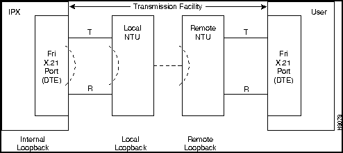
Local and remote loopbacks are available for all internode CDP-terminated connections. Local loopback exists at the system bus interface. It returns data and supervision back to the local facility to test the local CDP card, the associated BC-E1 or BC-T1 back card, and the customer connection. Remote loopback exists on the CDP card at the far end of the circuit and checks both directions of transmission on the network and much of the far CDP card.
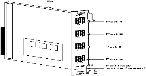
The CDP front panel has four LED indicators. These are ACTIVE, FAIL, MAJOR, and MINOR, as indicated in Table 1-17. The CDP monitors and reports statistics on the following input circuit line conditions:
Table 1-17 : CDP Front Panel Indicators
| Indicator | Meaning |
|---|---|
| ACTIVE (green) | On indicates card is active and carrying traffic. |
| FAIL (red) | On indicates self-test has detected a card failure in the main
card or optional integrated echo canceller board. |
| MAJOR (red) | A line failure has been detected locally on the receive side. |
| MINOR (yellow) | A line failure has been detected at the remote end. |
The CDP at each end of a connection is programmable for the two different voice encoding schemes. These encoding schemes are A-law and m-law, and they operate at E1 and T1 rates, respectively. Thus, the CDP supports international gateway applications. The CDP supports high-speed modem and FAX circuits. The CDP provides transparent, 64 Kbps. transport for CCS signalling. It also supports CAS signalling by transporting ABCD signalling transitions across the network with negligible distortion. The CDP can set, invert, and clear ABCD bits to accommodate some signalling conversions.
Echo cancellers are almost always required on voice circuits to compensate for the delays introduced with the various voice compression techniques used by the CDP. A built-in feature of the CDP is the on-board Integrated Echo Canceller (IEC). This eliminates having to provide this necessary feature with external equipment. Two models of the IEC are available: a 24-channel (T1) and a 31-channel (E1).
The CDP can provide data connections to the network. Data connections that originate on a CDP can terminate at another node on either a CDP, SDP, or LDP data card.
Data connections to the CDP fall into two categories: Superrate and Subrate. Superrate data connections are aggregates of channels that function as a single logical connection. These may be any multiple of 56 or 64 Kbps up to a maximum of 8 (512 Kbps). The DS0 timeslots must be contiguous or alternating (they cannot be random). All 56 Kbps data channels are bit-stuffed up to 64 Kbps on circuit lines but removed prior to packetization. Superrate connections do not carry supervisory bits.
Subrate data connections transmit at speeds less than 64 Kbps and are carried within a DS0. Allowable rates are: 2.4, 4.8, 9.6, and 56 Kbps. These are referred to as DS0A connections.
Inband DS0A link codes are translated into EIA control lead states for CDP to SDP or LDP connections, but fast EIA, DFM, and isochronous clocking are not available as with the SDP and LDP data cards.
A summary of the various types of connections supported by the CDP is provided in Table 1-18.
Table 1-18 : Types of Voice Circuits
| Type | Description |
|---|---|
| p | PCM only: A p-type connection carries 64 Kbps PCM voice and supports A-law or m-law encoding and conversion, level adjustment (gain/loss), and signalling. |
| t | Transparent: VF t-type connections carry 64 Kbps clear channel data traffics. |
| v | PCM and VAD: No ADPCM compression, but VAD enabled. Approximately 2:1 compression. |
| a16z
|
ADPCM. Standard 16 Kbps ADPCM only. Compressed code can have strings of zeros and must be used on lines that do not use ZCS (for example, that use B8ZS). |
| c16z | VAD and ADPCM. Uses a standard 16 Kbps ADPCM compression and Voice Activity Detection. Similar to a16z. Compressed code can have strings of zeros and must be used on lines that do not use ZCS (for example, that use B8ZS). |
| a32d
c32d |
ADPCM for FAX. The a32d and c32d circuit types are used for Enhanced Instafax. These types support high speed circuits but stay at 32 Kbps when a high-speed circuit is detected and thus support compression that would otherwise be unavailable. Unless a32d or c32d is selected, the circuit switches to 64 Kbps when a high-speed modem or FAX is detected on a voice circuit. This selection is made using the cnfvchparm command. The selection of a32d or c32d depends on the performance of the modem/FAX using the circuit and should be selected for error-free operation. |
| a32 a24 a16 | Uses ADPCM only. Can select 32 Kbps, 24 Kbps, or 16 Kbps compression. Compressed code avoids all zeros and can be used on lines with no other zero code suppression techniques. Modified 16 Kbps compression. |
| c32 c24 c16 | Uses both ADPCM and VAD. Can select 32 Kbps, 24 Kbps, or 16 Kbps for 2:1, 3:1 (approx.), or 4:1 ADPCM compression. Compressed code avoids all zeros and can be used on lines with no other zero code suppression techniques. 16 Kbps compression is non-standard. |
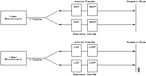
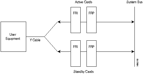
The CDP, BC-T1, BC-E1, BC-J1 can have a 1:1 redundancy configuration through a second, identical card set and a Y-cable to connect it to the trunk or circuit line. Figure 1-29 illustrates the redundant setup.
Figure 1-29 : Y-Cable Redundancy

The BC-J1 back card provides a Japanese J1 circuit line interface for a CDP card. The BC-J1 is a standard IPX back card and can reside in any rear slot 2-16 or 18-32 of the IPX node. The CDP must reside in the corresponding front slot. The front and back cards connect through the Local Bus (LB). The BC-J1 supports the following:
The BC-J1 supports two clock modes. These are normal clocking and loop timing. The system operator selects the mode through software control. Normal clocking uses the receive clock from the network for incoming data and supplies the transmit clock for outgoing data. This clock can be used to synchronize the node.
Loop timing uses the receive clock from the network for the incoming data and turns that same clock around for timing the transmit data.
Figure 1-30 and Table 1-19 show the controls and indicators on the BC-J1.
Figure 1-30 : BC-J1 Front Panel
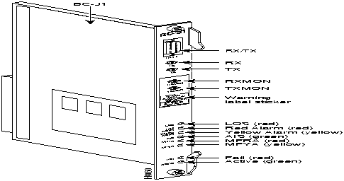
Table 1-19 : BC-J1 Connectors and Indicators
| No. | Connector/Indicator | Function |
|---|---|---|
| 1. | FAIL light (red) | Indicates that a failure has been detected on the card, and that the card cannot reliably carry data. The card must be replaced. |
| 2. | ACTIVE light (green) | Indicates that the card is in service and that active circuits are present. |
| 3. | LOS light (red) | Indicates loss of signal at the local end. |
| 4. | Red Alarm light (red) | Indicates loss of local frame alignment. |
| 5. | Yellow Alarm light (yellow) | Indicates loss of frame alignment at the remote end. |
| 6. | AIS light (green) | Indicates the presence of all ones on the line. |
| 7. | MFRA light (red) | Indicates loss of multiframe alignment |
| 8. | MFYA light (yellow) | Indicates loss of multiframe at the remote end |
| 9. | RX MON | BNC test connector for monitoring receive J1 line. |
| 10. | TX MON | BNC test connector for monitoring transmit J1 line. |
| 11. | RX-TX | Female DB15 connector for XMT and RCV J1. |
The TDM Transport Feature with the CDP
This section applies only to CDPs (and CVMs in the IGX) that have Rev. C firmware. Rev. C provides a service called Time Division Multiplexing Transport (TDM Transport). TDM Transport bundles DS0s to form a single, transparent connection through the network. TDM Transport is most valuable for transporting TDM data received from trunks in older, non-StrataCom WANs. For additional information, refer to the relevant commands in the Command Reference.
The Rev. C firmware features are as follows:
The limitations on TDM Transport within Rev. C firmware are as follows:
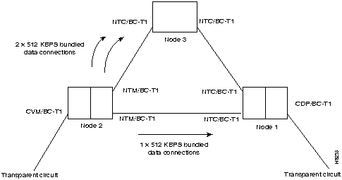
To achieve full T1 and E1 rates on a single CDP or CVM, TDM Transport supports inverse multiplexing. Figure 1-31 shows a simple example. In this example, the three, bundled 512-Kbps data connections symbolized by the arrows add up to a T1 connection.
Figure 1-31 : Inverse Multiplexing
Achieving Optimal Performance for TDM Transport
Because a single bit error can cause the entire group of connections to lose synchronization temporarily, trunks and nodes that carry the traffic should have a low bit error rate. To minimize the recovery time after a loss of synchronization, configure the least possible number of connections to carry the bandwidth. In specifying a transparent T1, for example, 3 8x64 connections is much better than 24 1x64 connections.
This section describes how to set up the Time Division Multiplexing Transport (TDM Transport) feature. Note that TDM Transport requires Rev. C firmware on all connected CVMs or CDPs that use this feature. Refer to the Command Reference for a description of the command parameters in related commands.
Before adding a bundled connection under TDM Transport, consider the following:
This section describes the front and back card sets for the standard and low-speed synchronous data interfaces.
Synchronous Data Interfaces with SDP/LDP
Synchronous data circuits have direct interfaces to the IPX by using either the SDP or LDP card set. The SDP set consists of a Synchronous Data Packet Assembler/Disassembler (SDP) front card and an associated Synchronous Data Interface (SDI) back card. The LDP set consists of the Low-speed Data Packet Assembler/Disassembler (LDP) and the Low-speed Data Interface (LDI) back card. The back cards are used to match the circuit type to the front data PAD card. Both card sets are listed in Table 1-20.
An IPX 16/32 node can have up to 25 SDP sets in a non-redundant system and thus supports up to 200 full-duplex data connections. An IPX 8 node can have up to 6 SDP sets in a non-redundant card configuration.
The IPX synchronous data cards support the ability to configure and monitor EIA leads; the ability to configure each channel for clocking, data rate, and DTE or DCE interface type; and complete loopback testing capability. Data channels can support null modem emulation as well as constant-carrier and switched-carrier operation. Data interfaces are protocol-transparent. Asynchronous, binary synchronous, and bit synchronous protocols are supported with no impact on host or terminal software.
Figure 1-32 : Synchronous Data Cards
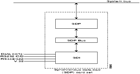
Table 1-20 : Synchronous Data PAD Cards Available
| Front Card | Back Card |
|---|---|
| SDP, Synchronous data PAD | SDI, RS-449 synchronous data interface (for X.21 or RS-422). |
| SDI, V.35 synchronous data interface. | |
| SDI, RS-232D synchronous data interface. | |
| SDI, RS-232C synchronous data interface (for V.24). | |
| LDP, Low speed data PAD | LDI, RS-232C (V.24) four-port and eight-port low-speed data interface, non-interleaved EIA. 4-port models limited to 56 Kbps, 8-port models up to 19.2 Kbps. |
| LDI, RS-232D four-port and 8-port, low-speed data interface, up to 19.2 Kbps., non-interleaved EIA. | |
| LDI4/DDS, four-port AT&T 56 Kbps Digital Data Service interface. |
Synchronous Data PAD Card (SDP)
The SDP front card in an IPX Data PAD group is a programmable communications processor that can support one to four medium speed, synchronous data channels. It operates at speeds from 1.2 Kbps up through 1.024 Mbps on all four ports while performing link error monitoring. Operation to 1.344 Mbps per port is permitted with link error monitoring disabled.
The SDP front data card:
An internal baud rate generator provides transmit and receive data clocks to the SDI card at the selected rate. The SDP can accept data from an external data device with a non-network synchronized clock (isochronous clock) up to 112 Kbps. With isochronous clocking, the SDP sends a clock control signal to the receiving end of the circuit to synchronize that SDP's receive clock to the isochronous clock received at the sending node.
Unless specified, a packet of data for EIA control lead information is built only at a very low rate or when a change of state is detected on one or more of the control leads. A fast EIA lead transmission can be specified in the software to send EIA control lead information in every FastPacket (interleaved EIA mode). This tightly couples the EIA lead states with the transmitted data but reduces the bandwidth efficiency.
The SDP synchronous data PAD card is installed in a front slot that has an SDP or UB-240 utility bus and an SDI back card. The SDI back card provides the proper data channel interface. The faceplate of the SDP/LDP has message lights and control buttons for loopback control and signal monitoring.
Synchronous Data Interface Card (SDI)
The SDI card is a synchronous data interface back card that must connect to a front SDP card via an SDP or UB-240 Utility Bus. Each SDI card has four connectors and provides the physical and electrical connection interface to four data ports. Each port configuration is the same as the other port configurations. One-for-one port redundancy is provided with a second card set and a standard Y-cable arrangement.
The SDI card provides:
Four types of SDI back cards can be used with an SDP front card to provide the data interface for customer data equipment. See Table 1-21 for a list of supported interfaces.
Table 1-21 : SDI Physical Interfaces
| Interface | No. of Ports | Connector Type |
|---|---|---|
| RS-232C/V.24 | 4-ports | DB25 Subminiature, female |
| RS-232D/V.24 | 4-ports | DB25 Subminiature, female |
| RS-449/X.21 | 4-ports | DB37 Subminiature, female |
| V.35 | 4-ports | 34-pin MRAC type (Winchester), female |
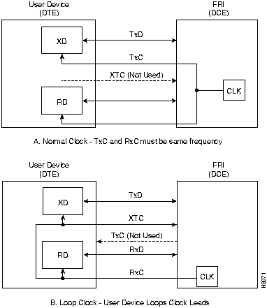
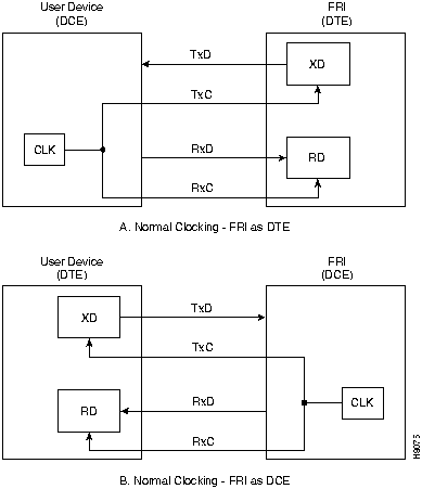
Three clocking modes are available with the SDI for clocking in transmit data and clocking out receive data. The three are normal clocking, loop clocking, and a split clock for transmission rates up to 112 Kbps. With loop clocking, the user device loops the RxC to the XTC for clocking out the transmit data.
In addition to the three clocking modes, the SDI can operate as either a DCE or DTE, which results in six combinations of clocking (See Figure 1-33 and Figure 1-34). The position of a jumper on the circuit side of the card determines the operational mode, and this is done upon system installation. All ports are configured together.
When the SDI is configured as a DTE, the user device is the source of clock timing and is generally not synchronous with the network (IPX) timing. This is referred to as isochronous clocking. Isochronous clocking allows the customer data sets at each end of a circuit to operate at slightly different rates (non-synchronously) with minimum delay and loss of data. This feature limits the amount of data allowed to accumulate in the SDP receive buffers and forces a re-synchronization when the delay approaches an unacceptable level.
Isochronous clocking operates at data rates up to 112 Kbps. It can be used on one input at a time per port. Therefore, it does not support two isochronous clock inputs in the same direction as required by modems that independently generate both TxC and RxC clocks.
Split clocking mode uses the user device timing for timing data transmission in one direction and the IPX timing for the other direction. The maximum rate is 112 Kbps.
Figure 1-33 : SDI (as DCE) Clocking Modes
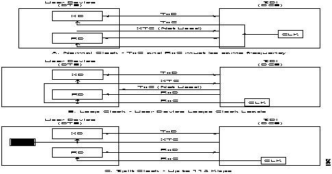
Figure 1-34 : SDI (as DTE) Clocking Modes
Two different utility buses have been used with the synchronous data cards. Earlier IPX systems have used an SDP Utility Bus to connect the SDP to the associated back card. The current bus that ships with SDP card sets is the 240-pin UB-240 Utility Bus. The UB-240 provides the same functionality as the 180-pin SDP Utility Bus but with greater noise immunity. The physical location of either of these buses is below the MUXBUS backplane.
The Low Speed Data PAD (LDP) front card is a low speed data PAD for use on RS-232C ports with data rates up to 19.2 Kbps. This programmable communications processor is a member of the IPX FastPacket Data PAD group and can support up to 8 synchronous or asynchronous data ports. When used with an LDI4/DDS, an LDP can provide 56-Kbps Digital Data Service (DDS) interfaces to the IPX. See Figure 1-35.
The LDP can process either synchronous or non-synchronous input data. For non-synchronous inputs, the data is over-sampled at a rate determined by how much data jitter the customer equipment can tolerate. Alternatively, a customer can use an external device to convert asynchronous data to synchronize data before the data goes to the IPX.
The LDP front data card:
Figure 1-35 : Low Speed Data PAD Card

A Model C or later LDP is required to support additional features such as embedded (fast) EIA, sixth EIA lead support, and pleisochronous clocking. In specifying the fast EIA control lead, the user can include the RTS/CTS EIA control leads in the same Fast Packet as customer data. The EIA control lead status is encoded as the eighth data bit in each data byte. This provides a quick EIA response without significantly affecting bandwidth requirements. It is limited to data rates of 19.2 Kbps. and below.
The LDP can go in any empty front slot. The LDP connects to an LDI back card over the LB Utility Bus. The faceplate of the LDP has message lights and control buttons for loopback control and signal monitoring. For more details, see Data Card Controls, Indicators and Connectors.
The ways in which LDP/LDI functionality is a subset of SDP/SDI functionality is as follows: the 4-port and 8-port LDPs support only a subset of the full RS-232C/D control leads. The LDP supports only non-isochronous DCE normal clocking and DCE or DTE looped clocking modes, transmission of 3 EIA lead states (non-interleaved), and baud rates of up to 19.2 Kbps. The LDI does not support split clock mode.
Low Speed Data Interface Card (LDI)
The Low-Speed Data Interface (LDI) card is the back card used with an LDP front card. Three models of LDI cards exist with either four or eight data ports as indicated in Table 1-22. The LDI provides the physical and electrical connection between the user low-speed data circuit and the LDP.
Some of the features of the LDI include:
Table 1-22 : LDI Physical Interfaces
| Unit | Interface | Ports | Connector Type |
|---|---|---|---|
| LDI 4 | RS-232C/D (V.24) | 4-ports | DB15 Subminiature, female |
| LDI 8 | RS-232C/D (V.24) | 8-ports | DB15 Subminiature, female |
| LDI 4 /DDS | DDS | 4-ports | DB15 Subminiature with pigtail adapter for 8-pin RJ-48 connections |
The LDI can operate either as DCE or DTE. A StrataCom DTE or DCE adapter cable between the port connector and the cable from the user device determines how the LDI operates. The cable is terminated with a standard DB25 on the customer end. Unlike the SDI, each port on the LDI is configured separately.
Three EIA control leads are brought out to the rear connectors. Three are used for DCE and three for DTE. Table 1-23 lists the function of these leads.
Table 1-23 : EIA Control Leads
| LDI as DCE | LDI as DTE |
|---|---|
| RTS | CTS |
| DSR | DTR |
| DCD | RL |
The remote loopback RL lead (sixth EIA lead) allows the use of a previously unused DTE EIA output lead. RL may be used to enable a far end modem loopback. Local loopback (LL) is not provided as an output on the LDI. If DTR is required, use the DTR lead by wiring it to the connector pin for local loopback.
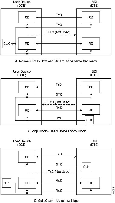
The two clocking modes that the LDI supports normal and looped (Figure 1-36). The normal mode is used when the LDI port is configured as a DCE. Looped clocking is used when the LDI port is configured as a DTE. The user device must take the external transmit clock and loop it back to the RxC for clocking in the receive date. In both cases, the LDI is the source of clock timing. Table 1-24 shows the accuracy and expected worst case jitter in an end-to-end circuit using LDIs at each end.
Table 1-24 : LDI Clocking Accuracy and Jitter Performance
| Baud Rate | Accuracy (± Hz.) | Jitter (±%) |
|---|---|---|
| 1200 | .06 | .03 |
| 2400 | .12 | .06 |
| 4800 | .24 | .12 |
| 9600 | .48 | .23 |
| 14,400 | .72 | .35 |
| 19,200 | .96 | .47 |
Figure 1-36 : LDI Clocking Modes
An LDI4/DDS card provides an interface for four 56-Kbps Digital Data Service (DDS) circuits for T1 service on IPX systems. The LDI4/DDS card can operate either as a Data Service Unit (DSU) or Office Channel Unit (OCU). It requires an LDP in the front slot. One for one port redundancy is available with a second card set and Y-cables for each port.
The LDI4/DDS operating parameters are software-selectable for DSU mode or OCU mode. Supported operating rates are: 2.4, 4.8, 9.6, 19.2, and 56 Kbps. Clock synchronization is looped clock for the OCU mode and external clock for the DSU mode. The LDI4/DDS supports the DDS control codes idle, zero suppression, out-of-service, and loopback sequences. The standard DDS diagnostic tools, such as local and remote loopbacks, are provided.
In the DSU mode, a port is connected to the local service provider. The service provider should guarantee that the line length does not cause more than the 34 dB loss limit specified by the DDS standard. For a port in the OCU mode, private wiring is used. In reference to OCU mode, see Table 1-25 for worst-case loss and maximum loop lengths for the different operating rates.
Table 1-25 : DDS Loop Length Maximums
| Line Rate | Loss | Equivalent Cable Length (miles) | |||
|---|---|---|---|---|---|
| (Kbps) | (dB) | 19 ga. | 22 ga. | 24 ga. | 26 ga. |
| 2.4 | 42 | 28.7 | 19.8 | 15.6 | 13.3 |
| 4.8 | 42 | 21.0 | 14.3 | 11.2 | 9.5 |
| 9.6 | 42 | 15.8 | 10.4 | 8.1 | 6.8 |
| 19.2 | 42 | 12.5 | 7.9 | 6.0 | 5.0 |
| 56 | 38 | 8.7 | 5.1 | 3.6 | 2.9 |
Data Card Controls, Indicators and Connectors
The SDP and LDP indicators and buttons are on the faceplate of the SDP and LDP (Figure 1-37 and Table 1-26). The buttons provide for loopback testing and for scrolling through the FastPacket data ports for a snapshot of selected data port conditions (indicated by PORT, PORT UNDER TEST, loopback, and communication line state lights).
The SDI comes only as a four-port card, whereas the LDI is available in either four-port or eight-port models. The appropriate connector type for the interface type is provided. See Figure 1-38.
Figure 1-37 : SDP and LDP Controls and Indicators
Figure 1-38 : SDI and LDI Connectors
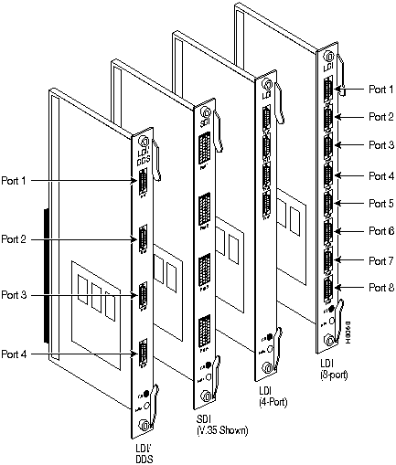
Table 1-26 : SDP and LDP Controls and Indicators
| No. | Indicator | Function |
|---|---|---|
| 1. | PORT light (yellow) | Indicates which FastPacket data port on the back card is currently under scrutiny. |
| 1A. | PORT Readout Display | Indicates which FastPacket data port (1 through 8) on the back card is currently under scrutiny. |
| 2. | SCROLL pushbutton | When pressed toggles through to the desired port. Information that is displayed by the remaining lights on the SDP and LDP front plate applies to the port whose corresponding light is ON. |
| 3. | LOOPBACK pushbutton | When pressed toggles through the three loopback states: no loopback, local loopback, and remote loopback. (This loopback is performed on the port whose corresponding light is ON.) |
| 4. | PORT UNDER TEST light
(yellow) |
Indicates that one of the ports has been placed in the loopback mode. If this is not the current port, press the SCROLL pushbutton to toggle in the port being tested. |
| 5. | LL light (yellow) | Indicates that a local loopback is occurring on one of the ports. |
| 6. | RL light (yellow) | Indicates that a remote loopback is occurring on one of the ports. |
| 7. | DTR light (green) | Indicates that the Data Terminal Ready signal is ON at the selected port terminal. |
| 8. | TXD light (green) | Indicates that the Transmit Data signal is ON at the selected port terminal. |
| 9. | DCD light (green) | Indicates that the Data Carrier Detect signal is ON at the selected port terminal. |
| 10. | RXD light (green) | Indicates that the Receive Data signal is ON at the selected port. |
| 11. | FAIL light (red) | Indicates that the card has failed. |
| 12. | ACTIVE light (green) | Indicates that the card is active and functioning normally. |
Optional redundancy for all data card types (SDP/SDI, LDP/LDI) can be provided with a second front and rear data card set and a Y-cable connection on each port to the customer data equipment. See Figure 1-39. The two front and back card pair sets must reside in adjacent shelf slots.
Figure 1-39 : Data Port Redundancy
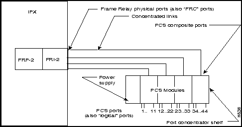
The IPX frame relay service is provided by a Frame Relay card set (FRP/FRI), and for expanded port capability, by a Port Concentrator Shelf that interfaces to a special Frame Relay Card set (FRP-2/FRI-2-X21). The Port Concentrator Shelf expands the number of ports provided by an FRP from 4 high-speed ports to 44 low-speed ports for applications requiring a higher density of frame relay ports at lower port speeds ranging from 9.6 to 384 Kbps. The high-speed capacity FRP/FRI Card set is described in Frame Relay Cards, and the Port Concentrator shelf is described in Port Concentrator Shelf (PCS).
Two protocols are used in frame relay service. The data transfer protocol operates end-to-end through the network. The LMI control protocol operates between the user device and the network.
The frame relay cards can provide a frame-forwarding service. This service forwards all valid HDLC frames from one port to a single, specified port elsewhere in the network without frame relay header processing or LMI control. Frame relay service also supports bundled connections and explicit congestion notification.
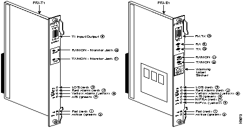
Frame Relay Cards (FRP and FRI)
A front card (FRP) and back card (FRI) make up the standard frame relay set (see Table 1-27). The card set can be installed in any shelf slot 2--31. These cards and associated software are optimized to accommodate the bursty nature of frame relay data without dedicating an overly large bandwidth to each circuit. The FRP-2 and FRI-X.21 cards and the Port Concentrator Shelf are described in Port Concentrator Shelf (PCS).
Table 1-27 : FRP-FRI Application
| Front Card Name | MIn. Model | Use With FRI
(Backcard Name) |
Min. Model |
|---|---|---|---|
| FRP---Frame Relay PAD Card | K
K |
V.35
X.21 |
B
A |
| FRP-6---Frame Relay PAD Card, w/6 can. | K | T1 or E1 | B (E1)
C (T1) |
| FRP-31---Frame Relay PAD Card, w/31 can. | K | T1 or E1 | B (E1)
C (T1) |
The Frame Relay PAD (FRP) front card is a programmable communications processor that can support one to four data ports. In single-port mode, it can run up to 2.048 Mbps. The FRP card requires an appropriate FRI back card. The following are FRP features.
All models of the FRP can process a maximum of 252 virtual circuits (PVCs). The PVCs can be distributed over the four ports in any manner as long as the total of 252 PVCs and a limit of 2.048 Mbps per FRP card is not exceeded. A node can support a maximum of 1024 PVCs---equivalent to four FRPs.
The FRP front card does the following:
The FRP converts frame relay data into Fast Packets and is transparent to the user data. Frame delimiting and transparency are provided by the HDLC flag bytes and bit stuffing. Valid hex 7E data bytes are converted using zero-bit insertion, so they are not mistaken for flag bytes.
On the receiving end, all frames are checked against the embedded Frame Check Sequence (FCS) code. Any frame that does not pass is discarded. Flag bytes that are used to fill up partially filled Fast Packet frames are also discarded.
If external clock is selected (hardware jumper in DTE position (V.35, X.21)), the FRP measures and reports the actual clock speed to the system software. Refer to Figure 1-41 for an illustration of each frame relay clocking type.
Any FRP model can support 252 virtual circuits or connections over any combination of ports.
Bundled and grouped connections are software groupings of multiple virtual circuits within a single routing connection. This allows a single node to support up to 1024 virtual circuits.
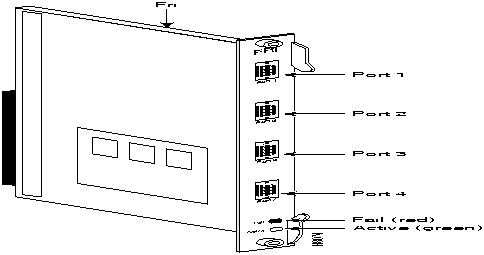
Frame Relay Interface (FRI) V.35 Card
The Frame Relay Interface V.35 (FRI-V.35) is a four-port back card to the FRP card. It requires a local bus to connect the FRI-V.35 and FRP to each other and to the System Bus. The two FRI-V.35 cards that can be used with the FRP are as follows:
The FRI-V.35 supports the following:
Figure 1-40 : Frame Relay V.35 Connectors and Indicators
FRI configurations support one to four ports. The configuration depends on the maximum required operating speed (the card itself has a maximum composite operating speed). Table 1-28 lists the available operating speeds for the combinations of FRP and FRI cards.
Table 1-28 : FRP/FRI-V.35 Operating Rates
| Port Speeds | FRP/FRI -V.35 MODELS | |||
|---|---|---|---|---|
| (Kbps) | A/A | B/A | C/A | C/B -D/B |
| 56 | X | X | X | X |
| 64 | X | X | X | X |
| 112 | X | X | X | X |
| 128 | X | X | X | X |
| 168 | X | X | X | X |
| 192 | X | X | X | X |
| 224 | X | X | X | X |
| 256 | X | X | X | X |
| 320 | X | |||
| 336 | X | X | X | |
| 384 | X | X | X | |
| 448 | X | X | X | |
| 512 | X | X | X | |
| 640 | X | |||
| 672 | X | X | X | |
| 768 | X | X | X | |
| 896 | X | X | X | |
| 960 | X | |||
| 1024 | X | X | X | X |
| 1280 | X | |||
| 1344 | X | |||
| 1536 | X | |||
| 1920 | X | |||
| 2048 | X | |||
Table 1-29 shows the relationship between the number of ports used on the FRI and the maximum operating speed for each port. Model A FRP and FRI cards are included for early users who may not have updated their cards.
Table 1-29 : Frame Relay Port Speed Combinations
| FRP/FRI MODELS | PORT 1 | PORT 2 | PORT 3 | PORT 4 |
|---|---|---|---|---|
| A/A | £ 256 | £ 256 | £ 256 | £ 256 |
| 1024 | 0 | 0 | 0 | |
| B/A | £ 256 | £ 256 | £ 256 | £ 256 |
| £ 336 | £ 336 | £ 336 | 0 | |
| £ 512 | £ 512 | 0 | 0 | |
| 1024 | 0 | 0 | 0 | |
| C/A | £ 256 | £ 256 | £ 256 | £ 256 |
| £ 336 | £ 336 | £ 336 | 0 | |
| £ 512 | £ 512 | 0 | 0 | |
| 1024 | 0 | 0 | 0 | |
| C/B
D/B |
Any one port may operate at either 2048 or 1920 Kbps. Any combination of ports may equal 2048 Kbps. If one port is 1920 Kbps, then no other port can be active. | |||
Frame Relay V.35 Port Numbering
Each frame relay port is assigned a number in the form:
SLOT is the slot number where the FRP/FRI-V.35 is located. PORT is the interface port in the range of 1-4. The top port on the FRI is port number 1. The DLCI is the destination Data Link Connection Identifier for the frame relay port. The DLCI can be any number in the range 1 through 1023.
The two clocking modes the FRI supports are normal and looped (Figure 1-41). In addition, the direction of the clock and data lines is reversed if the FRI is configured as a DCE or as a DTE, as follows:
Figure 1-41 : Frame Relay Data Clocking Modes This feature is a separate application of frame relay. The implementation of this feature requires three major components:
A Frame Relay T1/E1 connection can terminate on any Frame Relay Interface (V.35, X.21, T1 or E1, for example).
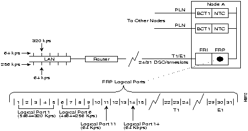
Frame Relay T1/E1 supports the grouping of FRP DS0/timeslots into "logical ports". These logical ports are either a single DS0/timeslot or groups of contiguous DS0/timeslots. Logical ports that consist of multiple DS0/timeslots are at the full rate of 64 Kbps per timeslot. Logical ports that consist of single DS0/timeslots can be configured 56 Kbps or 64 Kbps. See Figure 1-42.
If a logical port is configured for 56 Kbps, the IPX strips off the least significant bit (signalling bit) in the incoming octet and puts a "1" in the least significant bit of the outgoing octet. This 56 Kbps rate is typically used for groomed DDS circuits that appear on a T1/E1 line.
The features available for existing frame relay applications (LMI, 252 PVCs, and a full list of commands to gather statistics) are also available for Frame Relay T1/E1. The exceptions to this are external port loopbacks and signalling capability.
Figure 1-42 : Multiple and Single DS0s Forming a Logical Port Figure 1-43 : Frame Relay T1/E1 Cards and Indicators Port loopbacks towards the IPX (tstport and addextlp commands) are not supported. Port loopbacks towards the facility are supported using the addloclp and addrmtlp command.
Logical ports do not support supervisory-type signalling. There are no EIA leads or signalling bits as used in a V.35 port. The commands cnfict, cpyict, dspict and prtict are ignored unless an FRI V.35 back card is present. The dspbob command is blocked when executed on a logical port.
Frame Relay T1/E1 allows Y cable redundancy for FRI back cards. The Y-cable redundancy is not supported between differing back card types---FRI T1/E1 and FRI V.35, for example.
Inserting a back card that conflicts with a configured interface (upcln or upfrport) is flagged by a display of the back card in reverse video on the Y Cable Redundancy Screen.
Inserting a front card that does not support the number of upped ports is flagged by a display of the front card in reverse video on the Y-Cable Redundancy Screen.
A "Mismatch" error is displayed on the Card Status Screen (dspcd) when:
FRP front card Models A-D do not recognize FRI-T1/E1 back cards. The FRP Model E does not recognize FRI-V.35 back cards.
The Card Status Screen (dspcd) indicates the type of back card supported by the firmware on the FRP front card.
Commands for T1/E1 Frame Relay
The addfrport command creates logical ports. This command associates a group of DS0/timeslots to a logical port number. The lowest timeslot number of the created group becomes the logical port number. The logical port number is used to up the port (upfrport), add connections (addcon), and display statistics (dspportstats).
The dspfrport command displays logical ports in ascending port number sequence.
The delfrport command deletes logical ports. This command ungroups any multiple DS0/timeslots and/or unassigns a single DS0/timeslot logical port.
The FRI-X.21-type interface is included in the frame relay data ports supported by the IPX.
The operating rates of each port and the composite data rate supported by the FRI-X.21 card is the same as the frame relay V.35 card set. Each port may be configured either as a DCE or a DTE.
Frame Relay Interface (FRI) Card X.21
The Frame Relay Interface (FRI) back card used with the FRP front card provides the data port interface to the IPX network. Each FRI connects to a corresponding FRP and the System Bus via a Local Bus. The FRI-V.35 and FRI-X.21 are the two FRI cards available. They differ only in the physical interface they provide (see Table 1-30).
The FRI-X.21 applies to leased line service for international networks. The V.35 version applies to domestic U.S. use. The FRI is intended for connection to leased line service only and does not provide call control signalling support. All FRP models support the FRI-V.35, but the FRI-X.21 card is compatible with only the FRP Model F.
The FRI-X.21 back card supports:
The FRI can use one to four of its ports. The maximum required operating speed determines the number of ports used. Table 1-31 lists the available port operating speeds.
Any one port can operate at 2048 Kbps. Any combination of ports can equal 2048 Kbps. If one port is operating at 2048 Kbps, then no other port can be active. Port connectors are DB15 and are numbered 1 through 4. The top connector is port 1 (see Figure 1-44). Table 1-32 lists the cable and pinouts used for X.21 ports. Refer to the Command Reference Manual for further information.
Table 1-30 : FRI Card Types
Table 1-31 : Frame Relay Port Speeds Available
Table 1-32 : FRI-X.21 Port Pin Assignments (DB 15-connector)
Figure 1-44 : Frame Relay X.21 Connectors and Indicators The FRI-X.21 supports only normal clock mode. The direction of the clock and data lines depends on whether the FRI is configured as a DCE or a DTE as follows (see Figure 1-45):
Figure 1-45 : Frame Relay Data Clocking Modes Optional redundancy for the frame relay card types (FRP/FRI) can be provided with a second front and rear card set and a Y-cable connection on each of the four ports to the customer data equipment. See Figure 1-46. The two front and back card sets must reside in adjacent shelf slots.
A frame relay card redundancy option kit is available. It comes with a second FRP/FRI card set, a set of four Y-cables to interconnect the two card sets to the customer connection, and a redundant DCE/DTE programming board for the installed FRI. For conversion of a non-redundant card set to a redundant card set, the DCE/DTE daughterboard on the FRI must be changed.
After the hardware is installed, the node must be reconfigured to indicate that the slot has been set up for redundancy. Do this with the Add Y Redundancy (addyred) command. Refer to the Command Reference for more information on addyred.
Figure 1-46 : Frame Relay Port Redundancy Installation of the FRI-X.21 follows the same steps as other IPX back cards. It can be installed in any back slot except those slots normally reserved for the PCC/SCC (slots 1 and 2 for IPX 8 and IPX 16, slots 1 and 16 for IPX 32). The slot must be equipped with an LB1 Local Bus to provide interconnection between the FRI and FRP cards. The front card must be an FRP Model F, Revision C or later.
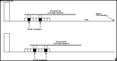
The four ports on the FRI are equipped with female 15-pin D sub miniature connectors. Each port may be configured as a DCE or as a DTE by selecting the position of a jumper board mounted on the FRI. The FRI ports are factory-configured as DCE interfaces.
If the interface configuration needs to be changed, reposition the jumper board for the FRI port(s), as follows:
Figure 1-47 : Positioning a DTE/DCE Block on an FRI-X.21 This section describes the steps for setting up a frame relay port after hardware installation. Port setup is performed from the IPX control terminal or StrataView Plus workstation. For details on each command used, refer to the IPX/BPX Command Reference Manual.
FRP/FRI Maintenance and Troubleshooting
This section describes the maintenance and troubleshooting features associated with the FRI-X.21 and FRP card set. No preventive maintenance is required.
As with all IPX cards, the FRI-X.21 includes a number of internal diagnostic routines that are periodically performed to test the card's performance. These diagnostics are automatically initiated and run in the background so as not to disrupt normal traffic. If a failure is detected during the self test, the front panel red FAIL LED is turned on. The status of the card may also be observed at the control terminal by using the Display Card (dspcd) command.
If a card failure is reported, it remains until cleared. A card failure is cleared by using the Reset Card (resetcd) command. The two types of resets that can be specified are hardware and failure history. The reset failure history clears the event log of any failure detected by the card selftest and does not disrupt card operation. Specifying a hardware reset performs a reset of the card firmware. A hardware reset reboots the firmware and momentarily disables the card. If a redundant card is available, the hardware reset causes activation of the standby card.
Card Testing with External Test Equipment
The FRP/FRI card set can be tested as a pair at the local node by using external test equipment such as a Bit Error Rate Tester (BERT). This can be useful in isolating "dribbling" error rates to either the cards, the frame relay data input, or the transmission facility. This test checks the data path from the electrical interface at the port through the card set to the MUXBUS in both directions of transmission.
To perform this test, proceed as follows:
The X.21 frame relay ports and any associated external modems, CSUs, or NTUs can be tested using data loopback points in the circuit path. Three possible loopbacks for X.21 frame relay ports may be established, as follows:
All three loopbacks are set up using the tstport command. Only one port at a time may be put in loopback mode for testing.
The internal loopback point is established inside the FRI card (see Figure 1-48). The FRP generates a test pattern, sends it out on the transmit circuitry, and detects this pattern on the receive circuitry. This test takes only several seconds and momentarily interrupts traffic on the port. It may be used for ports configured for either DCE or DTE.
Figure 1-48 : Frame Relay Loopback Modes For ports configured for DTE, two additional tests (local loopback and remote loopback) are available:
Replacing an FRI card is done the same way as an SDI card.
This section introduces the Port Concentrator Shelf (PCS). For more detailed information on the PCS, refer to the section on the Port Concentrator Shelf in the System Manual. For detailed installation instructions, refer to the Port Concentrator Installation document that comes with each unit. Cabling information for the PCS appears in the cabling appendix in the IPX Installation Guide and the Port Concentrator Installation document.
The PCS is an external device that expands the capacity of a Frame Relay Card to 44 low-speed ports. This ability to increase the port density of an IPX switch provides more efficient usage of the IPX card slots. The port parameters are as follows:
The PCS requires a version of the FRP/FRI card set that is exclusively dedicated to the PCS. The front card is the FRP-2. The back card that interfaces the FRP-2 to the PCS is the FRI-2-X.21. It provides one or more X.21 links. Each X.21 link is called a concentrated link. In a full configuration, each concentrated link services one of four 11-port modules in the PCS. This makes a total of 44 ports on the FRP-2.
Figure 1-49 : Port Concentrator Shelf Components The following terms are used to identify PCS components:
Other than front panel LEDs, the PCS has no user interface because the PCS functions as an extension of the FRP-2. PCS ports are operated and maintained from the IPX user interface.
The PCS operates within the IPX environment as a frame relay card with 44 ports. Existing frame relay commands (cnffrport, upfrport, dnfrport, addcon, delcon, etc.) are the same in syntax and function. The difference is that a range of 44 ports can be specified instead of 4. The configuration of each of the PCS logical ports is similar to that of non-PCS frame relay ports. A frame relay card connected to a PCS notifies the system database and permits the additional ports to be specified.
The PCS requires the following:
The concentrated link refers to the connection between the port concentrator and the frame relay card. Each PCS module supporting 11 external ports is connected to 1 of the 4 ports on the FRI-2-X.21 back card.
Each of the four composite links between PCS and IPX has a fixed configuration of:
The PCS Concentrated Link cable is illustrated in the cabling appendix. Its maximum length is 25 feet. The use of modems to extend this distance is not supported.
FRP-2 firmware interacts with the PCS over composite links only while the frame relay card is in an active state. The frame relay card changes from standby to active state when its first logical port is activated.
A PCS logical port associated with an FRP-2 card is activated with the upfrport command, as described in Frame Relay Connections chapter of the Command Reference.
You must know the slot number of the FRP-2 to which the PCS is connected; enter the slot number and a logical port in the range of 1-44 (assuming all four composites between the PCS and IPX connect).
Example: upfrport 4.1
This example indicates that the FRP-2 in slot 4 and concentrated link 1 are connected.
Entering the upfrport command for one port activates all four. The following events are generated by successful activation of four concentrated links. The display is from the example "upfrport 4.1:"
A noticeable delay occurs after upfrport begins executing on the first port. During initial upfrport execution, the FRP-2 performs first-time configuration, diagnostic, and up/download functions.
If a concentrated link is not connected or fails to come up, the logical port remains in a failed state until either the link comes up or the port is deactivated with the dnfrport command.
The frame relay card returns to the standby state after all 44 logical ports are de-activated with the dnfrport command.
When the frame relay ports are activated, the IPX recognizes them as PCS-connected ports. Subsequently, all applicable frame relay port management commands accept logical port numbers in the form slot.port. The range for port is 1-44.
The PCS supports the following logical ports, where <slot> is the IPX slot in which the FRP-2 is installed:
Table 1-33 : Links and Associated PCS Ports
Interface Hardware Configuration
The interface and clocking characteristics for each PCS port is independently configured to be V.11 (X.21), V.35, or V.28 by inserting the required interface card (or "ICARD") into the associated slot on the PCS module. For detailed information on PCS port hardware interfaces, refer to the Port Concentrator Installation document. This document comes in the PCS shipping container.
The IPX does not have the capacity to read the type of interface present for the PCS port. Values entered under the Interface Type parameter with the cnffrport command are used in the display only and cannot be checked against the hardware. Therefore, the correct value needs to be entered during port configuration.
A PCS is configured with the cnffrport command as described in the Frame Relay Connections chapter of the Command Reference. All parameters described in this section are supported with the following limitations:
All frame relay summary and interval statistics are kept for PCS ports.
The PCS and FRP-2 share responsibility for statistics collection on PCS ports. The PCS maintain counters for:
All remaining statistics counters are collected by the FRP-2. Although the IPX supports ForeSight for PCS connections, CLLM (ForeSight) statistics are not available in Release 8.1. These fields are present but not valid.
Monitoring functions generally apply to the PCS with the provision that up to 44 ports may be specified per FRP-2 slot. For descriptions of the monitoring commands, refer to the "Troubleshooting" chapter of the Command Reference. Note that commands dspchcnf, dspchstats, dspportstats, and dspbob fail when the required concentrated link is down. Trying to execute one of these commands on a concentrated link that is down causes an error message to appear.
Collection of Monitoring Information
The PCS measures the speed of receive data on logical ports if the port is configured as a DTE interface. To check the measured speed, use the dspbob command. The PCS measures port speed after any of the following occurs:
The process of measuring port speed sends out two 1-byte frames with no CRC on the port.
The IPX measures the physical port speed for FRI-2-X.21 ports once per minute. The current measured speed is displayed with the dspfrcport command and should always read 512 Kbps when the port is active.
Table 1-34 : PCS Module Front Panel LEDs
If the FRP-2 or FRI-2.X21 card is removed for any reason, be sure to maintain card compatibility upon card replacement: the FRP-2 card is compatible with only the FRI-2-X.21 back card. The IPX declares a mismatch state for any other back card inserted into an active FRP-2 slot. Inserting compatible hardware is the only way to clear the mismatch. Similarly, once an IPX slot is active with an FRP-2, a mismatch is declared if any other front card is inserted into this slot. Before the slot can be used for any other type of card, the slot must be de-activated as a PCS-capable frame relay card.
The commands in the list that follows apply to PCS frame relay ports. Most commands have the syntax described in the Command Reference with the provision that 44 ports per slot can be specified instead of 4.
A PCS logical port failure is defined as a Minor alarm. The FTC/FRP Port Comm Failure icon appears in the dspalms screen. Any connection that terminates on a failed port is also failed. Three causes of a port failure are defined, as described under Alarms and Events.
A failed connection on a PCS logical port is conditioned in the same manner as a failed connection on a non-PCS FRP port. Only the active control template is supported on PCS ports. The "conditioned" control template should not be used for PCS logical ports.
When it detects a Port Concentrator on one of its links, the FRP-2 checks for a compatible firmware revision on the Port Concentrator. If it detects incompatible firmware, the FRP-2 automatically downloads firmware to the Port Concentrator. This download operation takes about two minutes. An event is logged when a firmware download has either started or failed.
Operating software on the Port Concentrator is stored in Flash memory. Download should be required only if the PCS is connected to an FRP-2 with newer firmware, or a PCS module is replaced and a software version difference exists.
Automatic Diagnostics---FRP-2 and FRI-2-X.21 Cards
The FRP-2 card runs a self-test diagnostic when it is in the standby state. The system software uses a reserved channel on the FRP-2 card to perform background loopback tests that include both the FRP-2 and FRI-2-X.21. This test verifies that all components up to the FRI-2-X.21 physical port are functioning. These diagnostics do not test the PCS.
Information about PCS logical ports and frame relay connections is automatically reported to StrataView Plus, just as they are for FRP ports and connections.
Connection Management and other FRP-2 port functions may also be handled for PCS ports from StrataView Plus.
The SNMP agent supports Port Concentrator logical ports. This includes configuring PCS port parameters, adding, or deleting frame relay connections, and retrieving statistics.
The SNMP agent also supports provisioning for 44 frame relay ports for FRP-2; the existing MIB variables are extended to the expanded number of logical ports. SNMP management functions are not supported for the Port Concentrator concentrated links.
Interaction between the FRP-2 and PCS automatically updates the database to display the number of connected logical FRP-2 ports at the PCS. As a result, both the IPX user interface and the StrataView Plus interface automatically display the additional capacity of 44 ports for the FRP-2.
If, during normal operation, communication stops between FRP-2 and PCS over a concentrated link, a concentrated link failure alarm is generated.
In addition, during startup, a concentrated link is failed for any of the following reasons:
The FTC front card and FPC back card support the integration of FastPAD devices into an IPX network. The back card is available in both a V.35 and an X.21 version.
Each back card provides four ports. Each port can support one attached FastPAD device either locally or remotely via a modem. Dual card sets configured for Y-cable redundancy are supported.
When a FastPAD is attached to an IPX node, commands issued at the IPX control terminal provide card, port, FastPAD and connection management for the FTC/FPC card set and the attached FastPAD. Furthermore, statistics are collected for cards, ports, and the FastPAD and made available to StrataView Plus.
Card management of the FTC/FPC card set includes card installation and removal detection, card mismatch, and Y-cable redundancy.
Port management includes EIA signaling, LMI alarms, upping and downing of ports, and statistics generation for StrataView Plus.
FastPAD management permits the management of cards and ports on the FastPAD device from the IPX node. This management includes detection of card presence and card removal, card mismatch, and uploads and downloads between the FastPAD and the IPX node.
Connection management involves mapping FastPAD connections to Frame Relay type VCs (virtual circuits). Connections originating at a FastPAD must terminate at another FastPAD. Each FTC/FPC card set supports up to 252 VCs. VC statistics are collected and made available to StrataView Plus.
These new FastPAD management features became available by extending many IPX commands, such as addcon, cnfdclk, and cnfvchtp, to include FastPAD connections. In addition, certain new commands specific to FastPAD, for example, upftcport and addfp have been added. Refer to the IPX/BPX Command Reference Manual for details.
Installation of the FTC/FPC follows the same steps as other IPX card sets. Cards can be installed in any slot not reserved for the NPC/SCC. (A NPC/SCC can go in slots 1 and 2 for IPX 8 and IPX 16 or slots 1 and 16 for IPX 32.) The slot must be equipped with an LB1 Local Bus to provide interconnection between the FTC and FPC cards.
Each of the four ports on the FPC has a female, 15-pin D sub miniature connector. For each port on the FPC, a jumper position on a jumper board attached to the FPC configures an individual port as either DCE or a DTE. The default configuration for each port is DCE.
If the interface configuration needs changing, reposition the jumper board for the FPC port(s) by taking the following steps:
Figure 1-50 : Positioning a DTE/DCE Block on an FRI-X.21 Connectors, pin assignments, and card and port testing are identical to those of the corresponding frame relay back cards. Refer to Frame Relay Interface (FRI) V.35 Card for details of the V.35 backcard and Frame Relay FRI-X.21 for details of the X.21 back card.
This section provides an overview of the Alarm Relay card. The material includes a general description, features, equipment description, installation, and the modified user commands. Alarm summary outputs are provided by the alarm relay card set consisting of the ARC and ARI. This accommodates nodes equipped with only NTC and CDP cards to support relay contact alarm outputs.
Typically, the alarm outputs connect to a telephone central office alarm system for remote alarm reporting to indicate a problem in the associated equipment.
The alarm summary feature on the Alarm Relay cards provides both a visual, front panel indication of an IPX node alarm and a set of relay outputs for indicating node and network alarm indications. A visual alarm history indication is also provided.
The visual alarm history indication is an addition to the alarm output at the node's control port, which provides a data output to a control terminal (such as the StrataView Plus Network Management Station). Table 1-35 summarizes the alarm conditions and the resulting indications.
One set of alarm relays is used to display a major alarm or minor alarm for the node. One pair of contacts on each relay is used for audible alarms. These contacts are in series with a front panel alarm cut-off (ACO) switch. The other set of relay contacts is used for visual alarms. The ACO switch does not affect these contacts.
Any time the ACO switch is operated, a front panel ACO indicator is lit to remind the operator. If the ACO switch is operated to disable the node's audible alarm output and a second alarm arrives, the audible alarm is reactivated. Two front panel LEDs provide local indication of network major or minor alarms.
Table 1-35 : ARC Card Set Alarm Reporting
A second, independent set of alarm outputs exists to report network alarms. If either a major alarm or minor alarm occurs anywhere in the network, these alarm relays are activated.
Major alarm relays are normally energized (creating an open circuit), so a power failure at the node results in contact closure and a major alarm output. Minor alarms, however, are normally de-energized to conserve power, and both contact closures as well as contact openings are available for minor alarms.
When an alarm condition clears, the alarm relays return to their normal state to clear the alarm outputs. A front panel history indicator goes on whenever a node alarm occurs. The indicator remains on even though an alarm may have already cleared. The history indicator is manually cleared by pressing a front panel switch.
Two additional relays may be operated under software control to report any other condition. These are not utilized currently but may be defined in future releases.
The alarm reporting hardware and software requirements are as follows:
The alarm reporting feature requires a card set that includes an ARC front card, an ARI back card, and a UB-120 utility bus. This card set can go in any slot in the node except slot 1 (reserved for PCC or NPC). The recommended slot is slot 16 (the far right slot in the first or top shelf). Since a failure of either of these cards does not affect customer service, no provision exists for card redundancy.
Alarm Relay Card Description (ARC)
The alarm relays are controlled by the system software's Control Bus commands. The ARC card has an interface with the IPX Control Bus for receiving alarm signals from the NPC or NPC processor card and for sending status signals back to the processor card. It has no connection to the MUXBUS because no customer data exists for packetization. The firmware on the ARC card is responsible for alarm decoding.
The ARC front panel contains the alarm LEDs and ACO and History Clear push buttons as well as active and fail LEDs (for status of the ARC card). See Figure 1-51 and Table 1-36. The ARC card is used in conjunction with an ARI card and communicates with it by using a UB-120 Utility Bus. Relay drive signals originate in the ARC to operate relays on the ARI.
The ARC periodically runs a background self-test to determine the health of the card. If it fails a self-test, the front panel FAIL LED turns on, and the ACTIVE LED turns off.
Table 1-36 : ARC Front Panel Controls and Indicators
Alarm Relay Interface Description (ARI)
The Alarm Relay Interface (ARI) card contains the alarm relays and their associated drivers. A female DB37 connector on the faceplate provides the connection to the customer's office alarm or alarm reporting system. Refer to Figure 1-52 for an illustration of the ARI card and to Table 1-37 for the pinout of the connector. Table 1-38 lists the unassigned pins.
Alarm outputs are dry-contact closures or opening contacts from Form C relays. User-equipment must supply the voltage source to be switched by the IPX. Any source or load can be switched as long as it meets the following requirements.
Table 1-37 : ARI Alarm Connector Pin-Outs
Table 1-38 : Unassigned Connector Pins
Installation of an ARC card first requires removal of the node from service.
The ARC can go in any front slot except those slots normally reserved for the node processor cards. Reserved slots are 1 and 2 for the IPX 8/IPX 16 and slots 1 and 17 for the IPX 32. For standardization, the recommended slots are slot 8 in an IPX 8 and slot 16 in an IPX 16/32. The corresponding back slot must have an ARI card and a UB-120 Utility Bus.
To install an alarm card set, proceed as follows:
This section describes the steps required to set up an alarm card set after the physical installation. This is done from the IPX control terminal or StrataView Plus workstation. For details on each command used, see the IPX/BPX Command Reference Manual.
Maintenance and Troubleshooting
The paragraphs in this section describe the maintenance and troubleshooting features associated with the ARC card set. No preventive maintenance is required.
As with all IPX cards, the ARC includes a number of internal diagnostic routines that periodically run to test the card's performance. These diagnostics automatically run in the background and do not disrupt normal traffic. If a failure occurs during self-test, the front panel red FAIL LED goes on. The control terminal operator can observe card status by using the Display Card (dspcd) command. A report of a card failure remains until cleared. The Reset Card (resetcd) command clears the failure report.
The two types of resets that can be specified to resetcd are hardware and failure history. A reset failure history clears the event log of any failure detected by the card self-test and does not disrupt operation of the card. A reset of the card firmware is done by a hardware reset. A hardware reset reboots the firmware and momentarily disables the card.
Replacing an ARI card is done the same way as replacing an SDI card.
The following three commands apply to the ARC card set:
At least one IPX node in a network has a connection to either StrataView Plus, a control terminal, or a dial-in modem. Any control terminal connected in the network can configure, manage, monitor, and diagnose the entire network. In addition, at least one IPX node in a network may have an attached printer for printing error and event reports.
The control terminal and printer connect to two RS-232 serial ports (CONTrol port and AUXiliary Port). The RS-232 ports are located on the SCC faceplate. These serial ports support all standard asynchronous data rates from 1200 through 19,200 baud. The default rate is 9600 baud. Using the IPX software, data rates and the type of equipment connected to the ports can be configured.
To allow StrataCom Customer ISC personnel to perform remote diagnostic tests, a direct-dial modem attached to an IPX in the network is recommended. This modem connects to the midplane at the CONT port. In addition, an auto-dial modem can connect to the AUX port connector on the SCC at any node in the network so that remote error messages and alarms can be sent to the StrataCom ISC. The ISC automatically logs these messages.
Two external clock sources can connect to the SCC card through an external clock adapter cable. The external clock device can be either a 1.544 MHz or 2.048 MHz RS-422 square wave signal. The software-selectable choice depends on the primary application of the IPX. The clock stability should be at least as good as a STRATUM 3 clock source. Appendix B lists the terminals, printers, modems, and clock sources that have been tested and approved for the IPX.
Copyright 1988-1996 © Cisco Systems Inc.
Card Type
Interface
No. of Ports
Connector Type
FRI-X.21
X.21
4-ports
DB15 Sub miniature, female
FRI-V.35
V.35
4-ports
34-pin MRAC type (Winchester), female
Port Speeds (Kbps)
Maximum
Any multiple of 56 Kbps
Up to 1.792 Mbps
Any multiple of 64 Kbps
Up to 2.048 Mbps
Pin #
Name
Source
Description
1
Gnd.
both
Protective (Shield) ground
8
Sig. Gnd.
both
Signal ground
3/10
C
both
Control
5/12
I
both
Indication
2/9
TxD
DTE
Transmit Data from DTE
4/11
RxD
DCE
Receive Data to DTE
6/13
S
DCE
Clock Out (DCE), Clock In (DTE)
![]()
![]()

"Info FRP Port 4.1 Activated
"Info FRP Concentrated Link 4.1 Failure Cleared"
"Info FRP Concentrated Link 4.2 Failure Cleared"
"Info FRP Concentrated Link 4.3 Failure Cleared"
"Info FRP Concentrated Link 4.4 Failure Cleared"
PCS Ports
Composite L1
slot.1--slot.11
Composite L2
slot.12--slot.22
Composite L3
slot.23--slot.33
Composite L4
slot.34--slot.44
LED Name
Function
State
OFF = No power. RED = power applied but software not running.
GREEN = Operating software running.
Rx
Flashes for frames received on concentrated link.
With no activity on link, Link Rx blinks once per second.
With steady activity on link, Link Rx is on continuously.
Tx
Flashes for frames transmitted on concentrated link
With no activity on link, Link Tx blinks once per second.
With steady activity on link, Link Tx is on continuously.
CPU A
On solid when operating software on CPU A is running. Should always be On during operation.
CPU B
On solid when operating software on CPU B is running. Should always be On during operation.
Port 1
On for module connected to FRP-2 Port 1. Should always be On for Module 1.
Port 2
On for module connected to FRP-2 Port 2. Should always be On for Module 2.
Port 3
On for module connected to FRP-2 Port 3. Should always be On for Module 3.
Port 4
On for module connected to FRP-2 Port 4. Should always be On for Module 4.
Download
Flashes when frames are received during software download from FRP-2.
addcon
used to add frame relay connections.
addloclp
test command for creating local loopback.
addrmtlp
test command for creating remote loopback.
cnfcondsc
configures frame relay connection description.
cnfchpri
configures frame relay channel priority.
cnfchutl
optimizes frame relay channel utilization.
cnffrcls
configures frame relay class of service (also cnfcos command for connection).
cnffrcon
configures frame relay connection parameters.
cnffrport
configures frame relay port parameters.
cnfpref
configures preferred route for frame relay connection.
clrchstats
clears PCS frame relay channel statistics.
clrfrcportstats
PCS-specific command for clearing FRI-2-X.21 physical port statistics.
clrportstats
clears PCS frame relay port statistics.
delcon
deletes a frame relay connection.
delcongrp
deletes a frame relay connection group.
dellp
deletes a frame relay loopback condition.
dncon
deactivates a frame relay connection.
dspchcnf
displays channel configuration.
dspchstats
displays PCS frame relay channel statistics.
dspfrcportstats
PCS-specific command to display FRI-2-X.21 physical port statistics.
dspfrcbob
PCS-specific command for displaying FRI-2-X.21 physical port signals.
dspfrport
displays PCS logical port.
dspfrcport
displays FRI-2-X.21 physical port.
dsppcs
PCS-specific command to display PCS unit information.
dspportstats
displays PCS frame relay port statistics.
dspcon
displays frame relay connections.
prtcons
prints frame relay connections.
prtchcnf
prints frame relay channel configuration.
tstcon
tests frame relay connection.
tstdelay
tests frame relay connection delay.
tstpc
PCS-specific command to test the PCS.
resetpc
PCS-specific command to reset the PCS.
![]()
![]()
Alarm Category
Alarm Severity
Front Panel Indication
Relay Indication
Network
Major
none
Single form-C relay closure or opening.
Minor
none
Single form-C relay closure or opening.
Node
Major
MAJOR LED (red)
Visual and audible relay closure only (normally open).
Minor
MINOR LED (yellow)
Visual and audible form-C relay closure or opening.
Alarm Cutoff
n.a.
ACO LED (green)
Interrupts audible relay closure.
Alarm History
n.a.
HIST LED (green)
None.

No.
Indicator
Function
1.
MINOR LED (yellow)
Indicates a failure in the local node that is not service-affecting but still should be investigated. It could indicate problems such as a loss of redundancy, a low error rate on a digital trunk (frame bit errors or bipolar errors), etc.
2.
MAJOR LED (red)
Indicates a failure in the local node that is service-affecting and should be addressed immediately (an IPX card failure, for example).
3.
ACO LED (white)
Indicates that a MINOR or MAJOR alarm is present, and that the alarm cutoff (ACO) button (5) was pressed to silence an accompanying audible alarm. The ACO light is turned off when the alarm condition is cleared.
4.
HISTory light (green)
Indicates that an alarm has occurred sometime in the past on the node. The alarm may be current or it may have cleared. Pressing the HIST CLR button (6) turns off this light if there is no current alarm.
5.
ACO button
When pressed, this button silences audible alarm (visual alarms remain on) and turns on ACO light (3).
6.
HIST CLR button
When pressed, this button turns off HIST light (4) if there is no current alarm.
7.
FAIL light (red)
Indicates that the card has failed self-test.
8.
ACTIVE light (green)
Indicates that the card is active, has been assigned using the addalmslot command, and is functioning normally.

Pin #
Alarm Type
Alarm Name
Alarm Description
1
both
CHASSIS
Protective ground
3
Network
NWMAJA
Major---normally open contact
22
Network
Major---normally closed contact
4
Network
NWMAJC
Major---common contact
10
Node
MNVISA
Minor Visual---normally open contact
11
Node
Minor Visual---normally closed contact
12
Node
MNVISC
Minor Visual---common contact
16
Node
MJAUDC
Major Audible---common contact
17
Node
MJAUDA
Major Audible---normally open contact
23
Network
NWMINA
Minor---normally open contact
24
Network
Minor---normally closed contact
25
Network
NWMINC
Minor---common contact
29
Node
NWAUDA
Minor Audible---normally open contact
30
Node
Minor Audible---normally closed contact
31
Node
NWAUDC
Minor Audible---common contact
35
Node
MJVISC
Major Visual---common contact
36
Node
MJVISA
Major Visual---normally open contact
Pin #
Alarm Type
Alarm Description
7
Relay 2
common contact
8
Relay 2
normally closed contact
9
Relay 2
normally open contact
26
Relay 4
common contact
27
Relay 4
normally closed contact
28
Relay 4
normally open contact
![]()
Testing the operation of the alarm outputs involves creating an alarm and noting the corresponding alarm output. This can be done easily on a node that is not connected to the network but not for a node that is part of a normally operating network. The best time to create a major alarm is during a low traffic period. If this is done, proceed to Step 5. Otherwise, stop here.
![]()
![]()
![]()
![]()
![]()
![]()
![]()
![]()